


ADSP-TS201S
Rev. C | Page 9 of 48 | December 2006
LINK PORTS (LVDS)
The DSP’s four full-duplex link ports each provide additional
four-bit receive and four-bit transmit I/O capability, using low
voltage, differential-signal (LVDS) technology. With the ability
to operate at a double data rate—latching data on both the rising
and falling edges of the clock—running at up to 500 MHz, each
link port can support up to 500M bytes per second per direc-
tion, for a combined maximum throughput of 4G bytes
per second.
The link ports provide an optional communications channel
that is useful in multiprocessor systems for implementing point-
to-point interprocessor communications. Applications can also
use the link ports for booting.
Each link port has its own triple-buffered quad-word input and
double-buffered quad-word output registers. The DSP’s core
can write directly to a link port’s transmit register and read from
a receive register, or the DMA controller can perform DMA
transfers through eight (four transmit and four receive) dedi-
cated link port DMA channels.
Each link port direction has three signals that control its opera-
tion. For the transmitter, LxCLKOUT is the output transmit
clock, LxACKI is the handshake input to control the data flow,
and the LxBCMPO
output indicates that the block transfer is
complete. For the receiver, LxCLKIN is the input receive clock,
LxACKO is the handshake output to control the data flow, and
the LxBCMPI
input indicates that the block transfer is com-
plete. The LxDATO3–0 pins are the data output bus for the
transmitter and the LxDATI3–0 pins are the input data bus for
the receiver.
Applications can program separate error detection mechanisms
for transmit and receive operations (applications can use the
checksum mechanism to implement consecutive link port
transfers), the size of data packets, and the speed at which bytes
are transmitted.
TIMER AND GENERAL-PURPOSE I/O
The ADSP-TS201S processor has a timer pin (TMR0E) that
generates output when a programmed timer counter has
expired, and four programmable general-purpose I/O pins
(FLAG3–0) that can function as either single-bit input or out-
put. As outputs, these pins can signal peripheral devices; as
inputs, they can provide the test for conditional branching.
RESET AND BOOTING
The ADSP-TS201S processor has three levels of reset:
• Power-up reset – after power-up of the system (SCLK, all
static inputs, and strap pins are stable), the RST_IN
pin
must be asserted (low).
• Normal reset – for any chip reset following the power-up
reset, the RST_IN
pin must be asserted (low).
• DSP-core reset – when setting the SWRST bit in EMUCTL,
the DSP core is reset, but not the external port or I/O.
For normal operations, tie the RST_OUT
pin to the
POR_IN
pin.
After reset, the ADSP-TS201S processor has four boot options
for beginning operation:
• Boot from EPROM.
• Boot by an external master (host or another ADSP-TS201S
processor).
•Boot by link port.
• No boot—start running from memory address selected
with one of the IRQ3–0
interrupt signals. See Table 2.
Using the “no boot” option, the ADSP-TS201S processor must
start running from memory when one of the interrupts is
asserted.
The ADSP-TS201S processor core always exits from reset in the
idle state and waits for an interrupt. Some of the interrupts in
the interrupt vector table are initialized and enabled after reset.
For more information on boot options, see the EE-200:
ADSP-TS20x TigerSHARC Processor Boot Loader Kernels Oper-
ation on the Analog Devices website (www.analog.com).
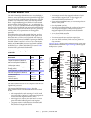
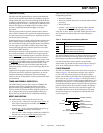
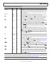
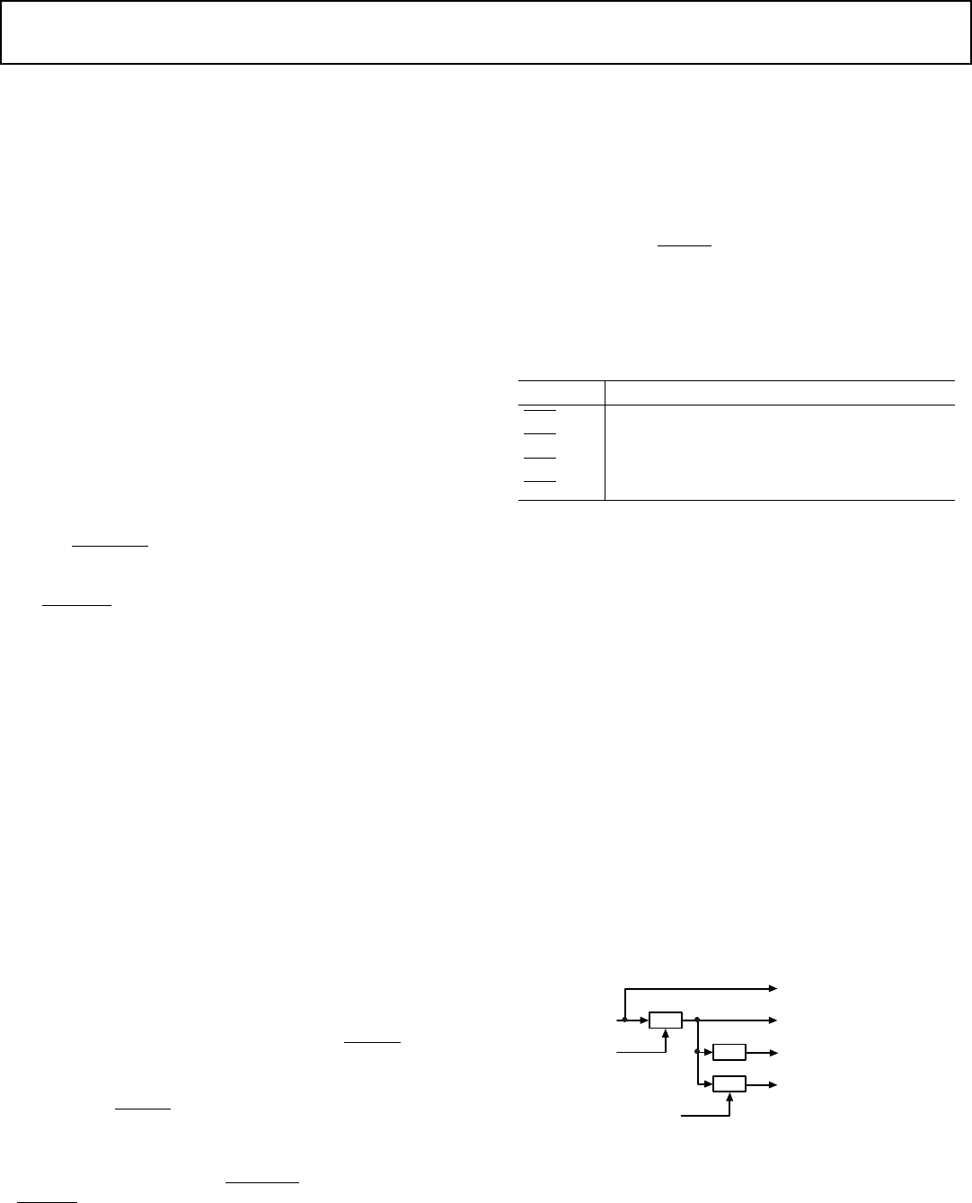
CLOCK DOMAINS
The DSP uses calculated ratios of the SCLK clock to operate, as
shown in Figure 5. The instruction execution rate is equal to
CCLK. A PLL from SCLK generates CCLK which is phase-
locked. The SCLKRATx pins define the clock multiplication of
SCLK to CCLK (see Table 4 on Page 12). The link port clock is
generated from CCLK via a software programmable divisor, and
the SOC bus operates at 1/2 CCLK. Memory transfers to exter-
nal and link port buffers operate at the SOCCLK rate. SCLK also
provides clock input for the external bus interface and defines
the ac specification reference for the external bus signals. The
external bus interface runs at the SCLK frequency. The maxi-
mum SCLK frequency is one quarter the internal DSP clock
(CCLK) frequency.
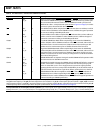
Table 2. No Boot, Run from Memory Addresses
Interrupt Address
IRQ0
0x3000 0000 (External Memory)
IRQ1
0x3800 0000 (External Memory)
IRQ2
0x8000 0000 (External Memory)
IRQ3
0x0000 0000 (Internal Memory)
Figure 5. Clock Domains
SCLKRATx
SCLK
SPD BITS,
LCTLx REGISTER
PLL
/2
/CR
CCLK
(INSTRUCTION RATE)
SOCCLK
(PERIPHERAL BUS RATE)
LxCLKOUT
(LINK OUTPUT RATE)
EXTERNAL INTERFACE