


Rev. C | Page 6 of 48 | December 2006
ADSP-TS201S
33.6G bytes per second, enabling the core and I/O to access
eight 32-bit data-words and four 32-bit instructions each cycle.
The DSP’s flexible memory structure enables:
• DSP core and I/O accesses to different memory blocks in
the same cycle
• DSP core access to three memory blocks in parallel—one
instruction and two data accesses
• Programmable partitioning of program and data memory
• Program access of all memory as 32-, 64-, or 128-bit
words—16-bit words with the DAB
EXTERNAL PORT
(OFF-CHIP MEMORY/PERIPHERALS INTERFACE)
The ADSP-TS201S processor’s external port provides the DSP’s
interface to off-chip memory and peripherals. The 4G word
address space is included in the DSP’s unified address space.
The separate on-chip buses—four 128-bit data buses and four
32-bit address buses—are multiplexed at the SOC interface and
transferred to the external port over the SOC bus to create an
external system bus transaction. The external system bus pro-
vides a single 64-bit data bus and a single 32-bit address bus.
The external port supports data transfer rates of 1G byte per
second over the external bus.
The external bus can be configured for 32-bit or 64-bit, little-
endian operations. When the system bus is configured for 64-bit
operations, the lower 32 bits of the external data bus connect to
even addresses, and the upper 32 bits connect to odd addresses.
The external port supports pipelined, slow, and SDRAM proto-
cols. Addressing of external memory devices and memory-
mapped peripherals is facilitated by on-chip decoding of high
order address lines to generate memory bank select signals.
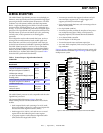
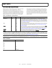
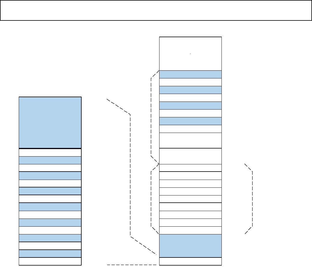
Figure 3. ADSP-TS201S Memory Map
RESERV ED
RE SERV ED
INTERNAL REGISTERS (UREGS)
INTERNAL MEMORY BLOCK 4
I NTE RNAL MEMORY BLOCK 2
I NTE RNAL MEMORY BLOCK 0
0x03 FFFFFF
0x001E0000
0x001E03FF
0x000DFFFF
0x000C0000
0x0009FFFF
0x00080000
0x0005FFFF
0x00040000
0x0001FFFF
0x00000000
INTERNAL SPACE
PROCESSOR ID 7
PROCESSOR ID 6
PROCESSOR ID 5
PROCESSOR ID 4
PROCESSOR ID 3
PROCESSOR ID 2
PROCESSOR ID 1
PROCESSOR ID 0
BROADCAST
HOS T (MSH)
BANK 1 (MS 1)
BANK 0 (MS 0)
MSSD BANK 0( MSSD0 )
INTERNAL MEMORY
0x50000000
0x40000000
0x38000000
0x30000000
0x2C000000
0x28000000
0x24000000
0x20000000
0x1C000000
0x18000000
0x14000000
0x10000000
0x0C000000
0x03FF FFFF
0x00000000
GLOBAL SPACE
0 xFFFFFFFF
M
U
L
T
IP
R
O
C
E
S
S
O
R
M
E
M
O
R
Y
S
P
A
C
E
E
X
T
E
R
N
A
L
M
E
M
O
R
Y
S
P
A
C
E
EACH IS A COP Y
OF INTERNAL SPACE
RESERV ED
INTERNAL MEMORY BLOCK 6
INTERNAL MEMORY BLOCK 8
0x0011FFFF
0x00100000
INTERNAL MEMORY BLOCK 10
0x0015FFFF
0x00140000
RESERV ED
RESERV ED
RESERV ED
RESERV ED
RESERV ED
RESERV ED
SOC REGISTER S (UREGS)
0x001F0000
0x001F03FF
MSSD BANK 1( MSSD1 )
MSSD BANK 2 (MSSD2)
MSSD BANK 3( MSSD3 )
0x60000000
0x70000000
0x80000000
RESER VED
RESER VED
RESER VED
RESER VED
0x54000000
0x44000000
0x64000000
0x74000000