


Rev. C | Page 16 of 48 | December 2006
ADSP-TS201S
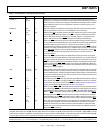
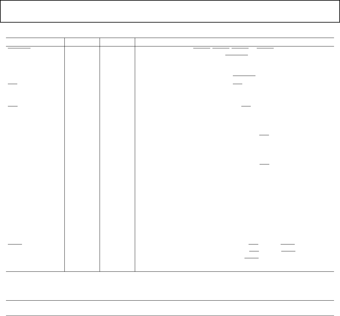
Table 8. Pin Definitions—External Port SDRAM Controller
Signal Type Term Description
MSSD3–0
I/O/T
(pu_0)
nc Memory Select SDRAM. MSSD0, MSSD1, MSSD2, or MSSD3 is asserted whenever the
DSP accesses SDRAM memory space. MSSD3–0 are decoded memory address pins
that are asserted whenever the DSP issues an SDRAM command cycle (access to
ADDR31:30 = 0b01—except reserved spaces shown in Figure 3 on Page 6). In a multi-
processor system, the master DSP drives MSSD3–0
.
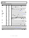
RAS
I/O/T
(pu_0)
nc Row Address Select. When sampled low, RAS indicates that a row address is valid in
a read or write of SDRAM. In other SDRAM accesses, it defines the type of operation
to execute according to SDRAM specification.
CAS I/O/T
(pu_0)
nc Column Address Select. When sampled low, CAS indicates that a column address is
valid in a read or write of SDRAM. In other SDRAM accesses, it defines the type of
operation to execute according to the SDRAM specification.
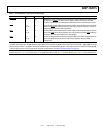
LDQM O/T
(pu_0)
nc Low Word SDRAM Data Mask. When sampled high, three-states the SDRAM DQ
buffers. LDQM is valid on SDRAM transactions when CAS
is asserted, and inactive on
read transactions. On write transactions, LDQM is active when accessing an odd
address word on a 64-bit memory bus to disable the write of the low word.
HDQM O/T
(pu_0)
nc High Word SDRAM Data Mask. When sampled high, three-states the SDRAM DQ
buffers. HDQM is valid on SDRAM transactions when CAS is asserted, and inactive on
read transactions. On write transactions, HDQM is active when accessing an even
address in word accesses or when memory is configured for a 32-bit bus to disable
the write of the high word.
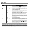
SDA10 O/T
(pu_0)
nc SDRAM Address Bit 10. Separate A10 signals enable SDRAM refresh operation while
the DSP executes non-SDRAM transactions.
SDCKE I/O/T
(pu_m/
pd_m)
nc SDRAM Clock Enable. Activates the SDRAM clock for SDRAM self-refresh or suspend
modes. A slave DSP in a multiprocessor system does not have the pull-up or pull-
down. A master DSP (or ID = 0 in a single processor system) has a pull-up before
granting the bus to the host, except when the SDRAM is put in self refresh mode. In
self refresh mode, the master has a pull-down before granting the bus to the host.
SDWE I/O/T
(pu_0)
nc SDRAM Write Enable. When sampled low while CAS is active, SDWE indicates an
SDRAM write access. When sampled high while CAS is active, SDWE indicates an
SDRAM read access. In other SDRAM accesses, SDWE defines the type of operation to
execute according to SDRAM specification.
I = input; A = asynchronous; O = output; OD = open-drain output; T = three-state; P = power supply; G = ground; pd = internal pull-down
5k
Ω; pu = internal pull-up 5 kΩ; pd_0 = internal pull-down 5 kΩ on DSP ID = 0; pu_0 = internal pull-up 5 kΩ on DSP ID = 0; pu_od_0 = internal
pull-up 500
Ω on DSP ID = 0; pd_m = internal pull-down 5 kΩ on DSP bus master; pu_m = internal pull-up 5 kΩ on DSP bus master; pu_ad
= internal pull-up 40 kΩ. For more pull-down and pull-up information, see Electrical Characteristics on Page 22.
Term (termination of unused pins) column symbols: epd = external pull-down approximately 5 k
Ω to V
SS
; epu = external pull-up approx-
imately 5 k
Ω to V
DD_IO
, nc = not connected; na = not applicable (always used); V
DD_IO
= connect directly to V
DD_IO
; V
SS
= connect directly to V
SS