


Rev. C | Page 18 of 48 | December 2006
ADSP-TS201S
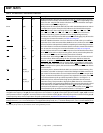
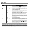
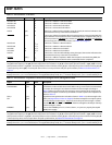
Table 11. Pin Definitions—Link Ports
Signal Type Term Description
LxDATO3–0P O nc Link Ports 3–0 Data 3–0 Transmit LVDS P
LxDATO3–0N O nc Link Ports 3–0 Data 3–0 Transmit LVDS N
LxCLKOUTP O nc Link Ports 3–0 Transmit Clock LVDS P
LxCLKOUTN O nc Link Ports 3–0 Transmit Clock LVDS N
LxACKI I (pd) nc Link Ports 3–0 Receive Acknowledge. Using this signal, the receiver indicates to the
transmitter that it may continue the transmission.
LxBCMPO
O (pu) nc Link Ports 3–0 Block Completion. When the transmission is executed using DMA, this
signal indicates to the receiver that the transmitted block is completed. The pull-up
resistor is present on L0BCMPO
only. At reset, the L1BCMPO, L2BCMPO, and L3BCMPO
pins are strap pins. For more information, see Table 16 on Page 20.
LxDATI3–0P I V
DD_IO
Link Ports 3–0 Data 3–0 Receive LVDS P
LxDATI3–0N I V
DD_IO
Link Ports 3–0 Data 3–0 Receive LVDS N
LxCLKINP I/A V
DD_IO
Link Ports 3–0 Receive Clock LVDS P
LxCLKINN I/A V
DD_IO
Link Ports 3–0 Receive Clock LVDS N
LxACKO O nc Link Ports 3–0 Transmit Acknowledge. Using this signal, the receiver indicates to the
transmitter that it may continue the transmission.
LxBCMPI
I (pd_l) V
SS
Link Ports 3–0 Block Completion. When the reception is executed using DMA, this
signal indicates to the receiver that the transmitted block is completed.
I = input; A = asynchronous; O = output; OD = open-drain output; T = three-state; P = power supply; G = ground; pd = internal pull-down
5k
Ω; pu = internal pull-up 5 kΩ; pd_0 = internal pull-down 5 kΩ on DSP ID = 0; pu_0 = internal pull-up 5 kΩ on DSP ID = 0; pu_od_0 = internal
pull-up 500
Ω on DSP ID = 0; pd_m = internal pull-down 5 kΩ on DSP bus master; pu_m = internal pull-up 5 kΩ on DSP bus master; pu_ad
= internal pull-up 40 kΩ; pd_l = internal pull-down 50 kΩ. For more pull-down and pull-up information, see Electrical Characteristics on
Page 22.
Term (termination of unused pins) column symbols: epd = external pull-down approximately 5 k
Ω to V
SS
; epu = external pull-up approx-
imately 5 k
Ω to V
DD_IO
, nc = not connected; na = not applicable (always used); V
DD_IO
= connect directly to V
DD_IO
; V
SS
= connect directly to V
SS
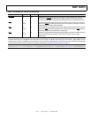
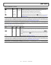
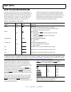
Table 12. Pin Definitions—Impedance Control, Drive Strength Control, and Regulator Enable
Signal Type Term Description
CONTROLIMP0
CONTROLIMP1
I (pd)
I (pu)
na
na
Impedance Control. As shown in Table 13, the CONTROLIMP1–0 pins select between
normal driver mode and A/D driver mode. When using normal mode (recommended),
the output drive strength is set relative to maximum drive strength according to
Table 14. When using A/D mode, the resistance control operates in the analog mode,
where drive strength is continuously controlled to match a specific line impedance as
shown in Table 14.
DS2, 0
DS1
I (pu)
I (pd)
na Digital Drive Strength Selection. Selected as shown in Table 14. For drive strength calcu-
lation, see Output Drive Currents on Page 36. The drive strength for some pins is preset,
not controlled by the DS2–0 pins. The pins that are always at drive strength 7 (100%)
include: CPA, DPA, TDO, EMU, and RST_OUT. The drive strength for the ACK pin is always
x2 drive strength 7 (100%).
ENEDREG I (pu) V
SS
Connect the ENEDREG pin to V
SS
. Connect the V
DD_DRAM
pins to a properly decoupled
DRAM power supply.
I = input; A = asynchronous; O = output; OD = open-drain output; T = three-state; P = power supply; G = ground; pd = internal pull-down
5k
Ω; pu = internal pull-up 5 kΩ; pd_0 = internal pull-down 5 kΩ on DSP ID = 0; pu_0 = internal pull-up 5 kΩ on DSP ID = 0; pu_od_0 = internal
pull-up 500
Ω on DSP ID = 0; pd_m = internal pull-down 5 kΩ on DSP bus master; pu_m = internal pull-up 5 kΩ on DSP bus master; pu_ad
= internal pull-up 40 k
Ω. For more pull-down and pull-up information, see Electrical Characteristics on Page 22.
Term (termination of unused pins) column symbols: epd = external pull-down approximately 5 k
Ω to V
SS
; epu = external pull-up approx-
imately 5 k
Ω to V
DD_IO
, nc = not connected; na = not applicable (always used); V
DD_IO
= connect directly to V
DD_IO
; V
SS
= connect directly to V
SS