


ADSP-TS201S
Rev. C | Page 25 of 48 | December 2006
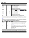
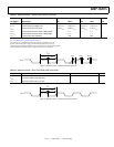
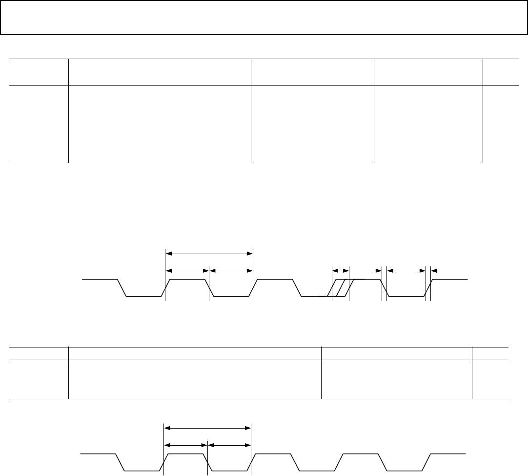
Table 23. Reference Clocks—System Clock (SCLK) Cycle Time
Parameter Description
SCLKRAT = 4×, 6×, 8×, 10×, 12× SCLKRAT = 5×, 7×
UnitMin Max Min Max
t
SCLK
1, 2, 3
System Clock Cycle Time 8 50 8 50 ns
t
SCLKH
System Clock Cycle High Time 0.40 × t
SCLK
0.60 × t
SCLK
0.45 × t
SCLK
0.55 × t
SCLK
ns
t
SCLKL
System Clock Cycle Low Time 0.40 × t
SCLK
0.60 × t
SCLK
0.45 × t
SCLK
0.55 × t
SCLK
ns
t
SCLKF
System Clock Transition Time—Falling Edge
4
—1.5—1.5ns
t
SCLKR
System Clock Transition Time—Rising Edge — 1.5 — 1.5 ns
t
SCLKJ
5, 6
System Clock Jitter Tolerance — 500 — 500 ps
1
For more information, see Table 3 on Page 12.
2
For more information, see Clock Domains on Page 9.
3
The value of (t
SCLK
/ SCLKRAT2-0) must not violate the specification for t
CCLK
.
4
System clock transition times apply to minimum SCLK cycle time (t
SCLK
) only.
5
Actual input jitter should be combined with ac specifications for accurate timing analysis.
6
Jitter specification is maximum peak-to-peak time interval error (TIE) jitter.
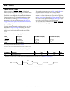
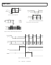
Figure 10. Reference Clocks—System Clock (SCLK) Cycle Time
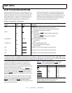
Table 24. Reference Clocks—JTAG Test Clock (TCK) Cycle Time
Parameter Description Min Max Unit
t
TCK
Test Clock (JTAG) Cycle Time Greater of 30 or t
CCLK
× 4 — ns
t
TCKH
Test Clock (JTAG) Cycle High Time 12 — ns
t
TCKL
Test Clock (JTAG) Cycle Low Time 12 — ns
Figure 11. Reference Clocks—JTAG Test Clock (TCK) Cycle Time
SCLK
t
SCLK
t
SCLKH
t
SCLKL
t
SCLKJ
t
SCLKF
t
SCLKR
TCK
t
TCK
t
TCKH
t
TCKL