


Rev. C | Page 34 of 48 | December 2006
ADSP-TS201S
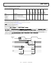
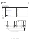
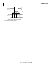
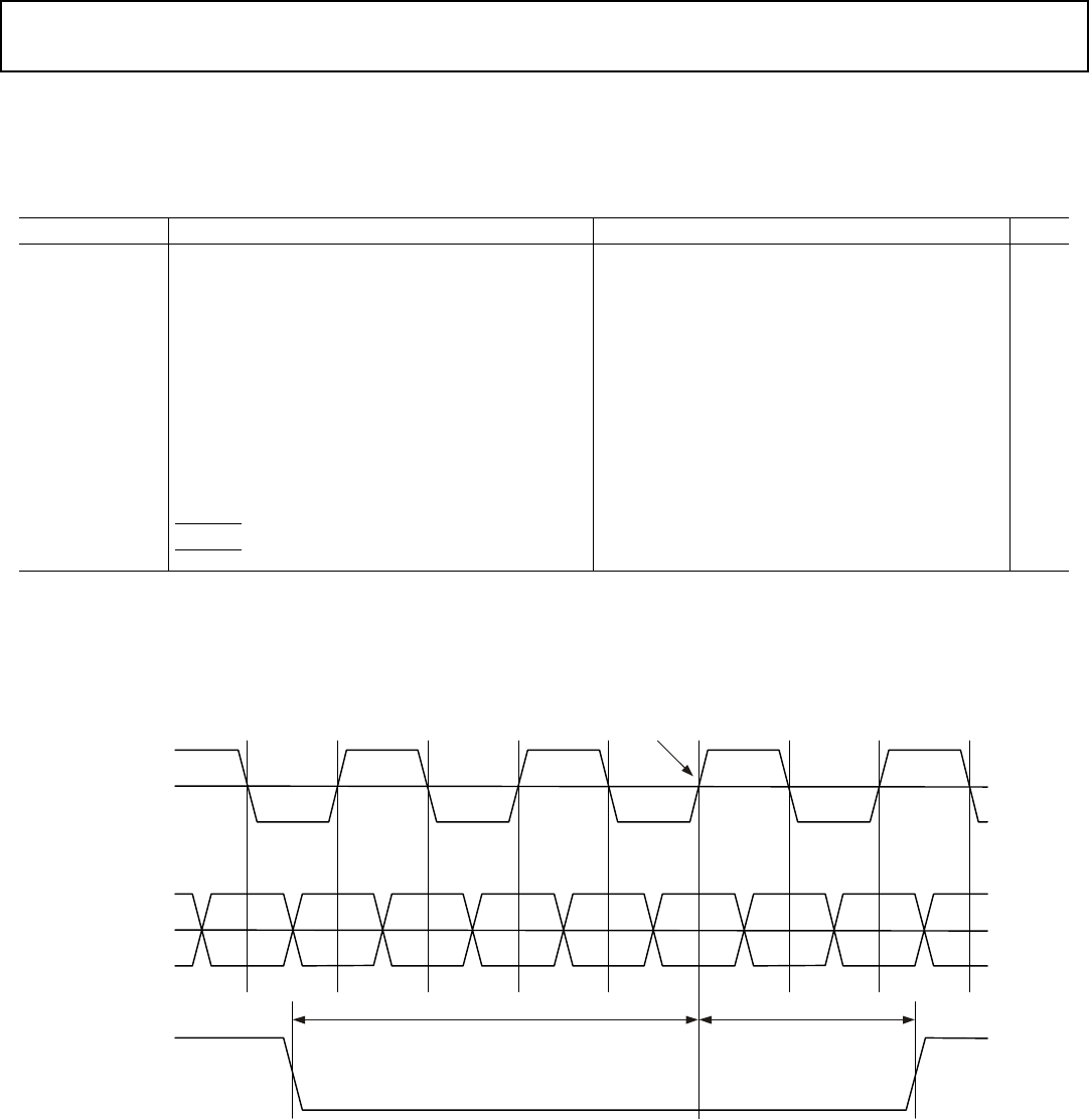
Link Port—Data In Timing
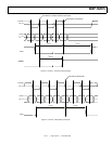
Table 33 with Figure 24 and Figure 25 provide the data in
timing for the LVDS link ports.
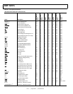
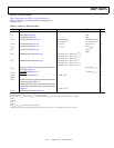
Table 33. Link Port—Data In Timing
Parameter Description Min Max Unit
Inputs
t
LCLKIP
LxCLKIN Period (Figure 25)Greater of 1.8
or 0.9 × t
CCLK
1
12.5 ns
t
LDIS
LxDATI Input Setup (Figure 25)0.20
1,
2
0.25
1,
3
0.30
1,
4
0.35
1,
5
ns
ns
ns
ns
t
LDIH
LxDATI Input Hold (Figure 25)0.20
1, 2
0.25
1, 3
0.30
1, 4
0.35
1, 5
ns
ns
ns
ns
t
BCMPIS
LxBCMPI Setup (Figure 24)2×t
LCLKIP
1
ns
t
BCMPIH
LxBCMPI Hold (Figure 24)2×t
LCLKIP
1
ns
1
Timing is relative to the 0 differential voltage (V
OD
= 0).
2
|V
ID
| = 250 mV
3
|V
ID
| = 217 mV
4
|V
ID
| = 206 mV
5
|V
ID
| = 195 mV
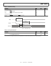
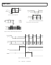
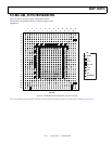
Figure 24. Link Ports—Last Received Quad Word
LxCLKIN
LxDATI
V
OD
=0V
V
OD
=0V
t
BCMPIS
LxBCMPI
t
BCM P IH
FIRST EDGE IN FIFTH SHORT WORD IN A QUAD WORD