


ASUS A7V266-MX motherboard user guide
2-15
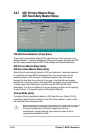
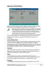
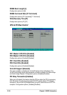
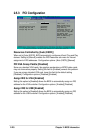
DRAM Clock/Drive Control
DRAM Timing [Safe]
DRAM CAS Latency [2.5]
Bank Interleave [Disabled]
Pre-charge to Active (Trp) [2T]
Active to CMD (Trcd) [2T]
DRAM Burst Lenght [4]
DRAM Command Rate [2T Command]
Write Recovery Time [3T]
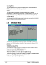
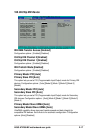
DRAM Clock/Drive Control
Press [Enter] to
select DRAM Timing
Mode. [Safe] is
recommended. [Manual]
allows you to set each
configuration on your
own.
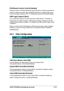
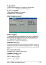
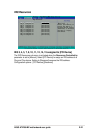
TV_Type [NTSC]
This option allows you to select the TV standard for TV display output.
Configuration options: [NTSC] [PAL] [PALM] [PALN] [PALNc]
TV_Connector [CVBS]
This item allows you to select the TV connector.
Configuration options: [CVBS] [S-Video 0]
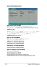
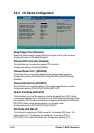
DRAM Timing [Safe]
It is recommended that you set this parameter to [Safe]. Setting to [Auto by SPD]
synchronizes the DRAM timing with the DRAM Clock. Setting to [Manual] allows
you to set the values for DRAM CAS Latency, Bank Interleave, Pre-charge to
Active (TRP) and Active to CMD (Trcd) prameters.
Configuration options: [Safe] [Auto By SPD] [Manual]
DRAM CAS Latency [2.5]
This field sets the override clock cycle for the latency time between the DRAM read
command and the moment that the data actually becomes available. Normally, the
system determines the rate automatically by default. Configuration options: [1.5] [2]
[2.5] [3]
Bank Interleave [Disabled]
Configuration options: [Disabled] [2 Bank] [4 Bank]
Precharge to Active (Trp) [2T]
Configuration options: [2T] [3T]
Active to CMD (Trcd) [2T]
Configuration options: [2T] [3T]