


2-16
Chapter 2: BIOS Information
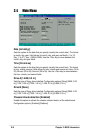
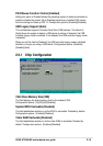
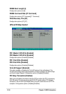
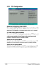
CPU & PCI Bus Control
PCI1 Master 0 WS Write [Enabled]
PCI2 Master 0 WS Write [Enabled]
Configuration options: [Enabled] [Disabled]
PCI1 Post Write [Enabled]
PCI2 Post Write [Enabled]
Configuration options: [Enabled] [Disabled]
VLink 8X Support [Enabled]
This option enables or disables the VLink 8X feature of the motherboard. The
VLink 8X technology allows high bandwidth connection between the North bridge
and South bridge chipsets. Configuration options: [Enabled] [Disabled]
PCI Delay Transaction [Enabled]
When set to [Enabled], this feature frees the PCI bus when the CPU is accessing
8-bit ISA cards. This process consumes 50-60 PCI clocks without PCI delayed
transaction. Set this field to [Disabled] when using ISA cards that are not PCI 2.2
compliant. Configuration options: [Enabled] [Disabled]
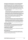
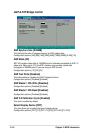
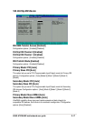
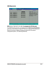
PCI1 Master 0 WS Write [Enabled]
PCI2 Master 0 WS Write [Enabled]
PCI1 Post Write [Enabled]
PCI2 Post Write [Enabled]
VLink 8X Support [Enabled]
PCI Delay Transaction [Enabled]
CPU & PCI Bus Control
Press [Enter] to
select [Enabled] or
[Disabled].
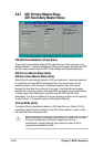
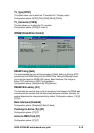
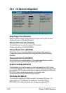
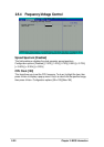
DRAM Burst Lenght [4]
Configuration options: [4] [8]
DRAM Command Rate [2T Command]
Configuration options: [2T Command] [1T Command]
Write Recovery Time [3T]
Configuration options: [3T] [2T]