


— iv —
APPENDIX
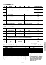
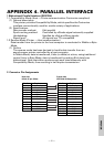
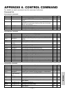
3. Connector Pin Configuration
Source
Host
Host/Ptr
Host/Ptr
Host/Ptr
Host/Ptr
Host/Ptr
Host/Ptr
Host/Ptr
Host/Ptr
Printer
Printer
Printer
Printer
Host
Printer
Host
Printer
GND
Printer
Printer
Host
Pin
1
2
3
4
5
6
7
8
9
10
11
12
13
14
15
16
17
18
19—30
31
32
33
34
35
36
Compatibility Mode
nStrobe
Data0(LSB)
Data1
Data2
Data3
Data4
Data5
Data6
Data7
nAck
Busy
PEerror
Select
nAutoFd
NC
GND
FG
Logic-H
GND
Init
nFault
GND
DK_STATUS
+5V
nSelectIn
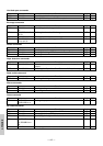
Nibble Mode
HostClk
Data0(LSB)
Data1
Data2
Data3
Data4
Data5
Data6
Data7
PtrClk
PtrBusy/Data3.7
AckDataReq/Data2.6
Xflag/Data1.5
HostBusy
ND
GND
FG
Logic-H
GND
Init
nDataAvail/Data0.4
ND
ND
ND
1284-Active
Byte Mode
HostClk
Data0(LSB)
Data1
Data2
Data3
Data4
Data5
Data6
Data7
PtrClk
PtrBusy
AckDataReq
Xflag
HostBusy
ND
GND
FG
Logic-H
GND
Init
nDataAvail
ND
ND
ND
1284-Active
NC: Not Connected
ND: Not Defined
Applicable connectors: Printer side: 57LE-40360 (Amphenol or equivalent)
Cable side: 57-30360 (Amphenol or equivalent)
CAUTION
• The first letter “n” of each signal name indicates that the signal is active “L”. If any one of
the above signals is not available, bidirectional communication cannot be accomplished.
• In interfacing signals, be sure to use twist-paired wires for signal lines, and the return side
must be connected to signal ground level. All interfacing conditions are specified based on
C-MOS level and must satisfy the following characteristics. Also, specify the rising and
falling time of each signal as 0.5 µs.
• Avoid transferring data by ignoring nAck or Busy signal; otherwise, the data may be erased.
Make the interface cables as short as necessary.
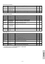
4. Electrical Characteristics
4.1 Input and output conditions
All the input signals, DATA 0-7, are each pulled up with 50 KΩ resistor, and the other
input signals are each pulled up with a 3.3 KΩ resistor.
The DK_STATUS signal is set to “High” if the Drawer switch is open, and set to
“Low” if the switch is closed. The +5V signal is pulled up through a 3.3KΩ resistor.
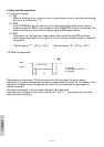
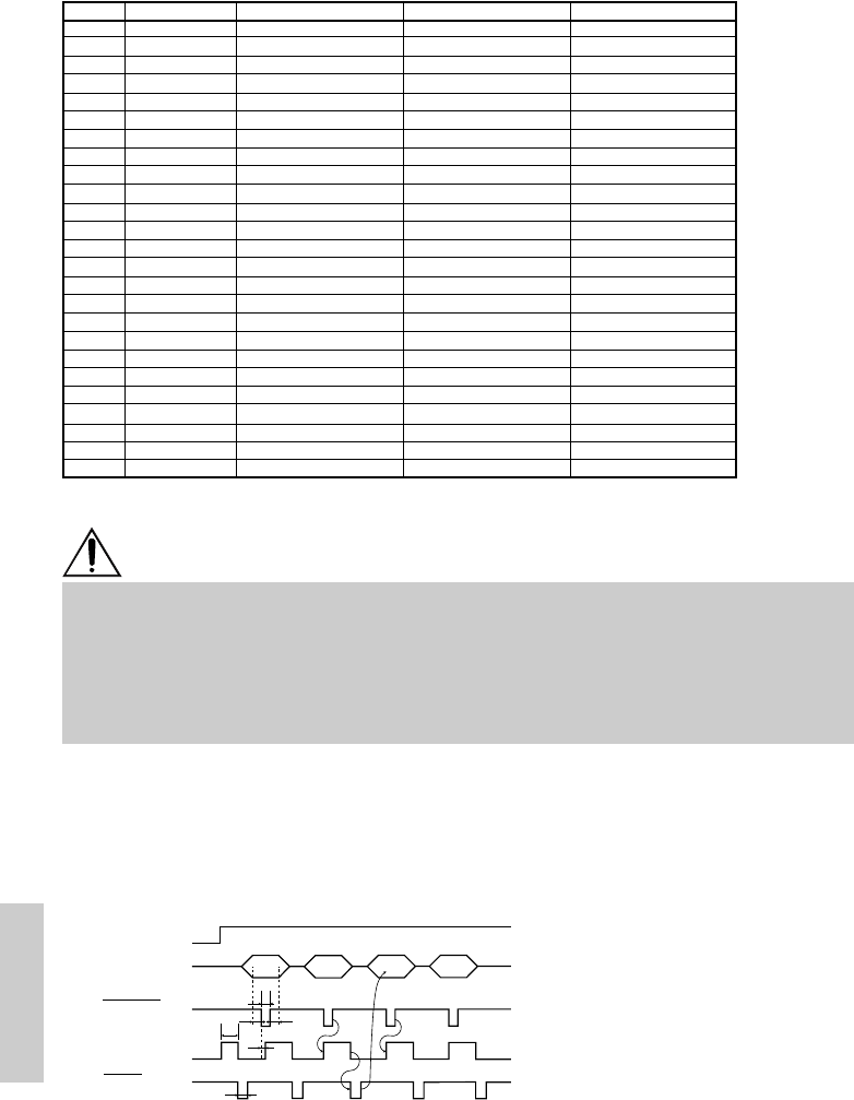
4.2 Timing Chart (Compatibility Mode)
T1, T2, T3: 0.5 µs MIN
T4: 270 ns MAX
T5: 2.3 µs TYP
T6: 500 ms MIN (At power-on)
T6
T1
T3
T2
T4
T5
Power
nStrobe
Data
Busy
nAck