20 Jackrabbit (BL1800)
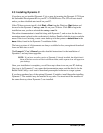
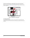
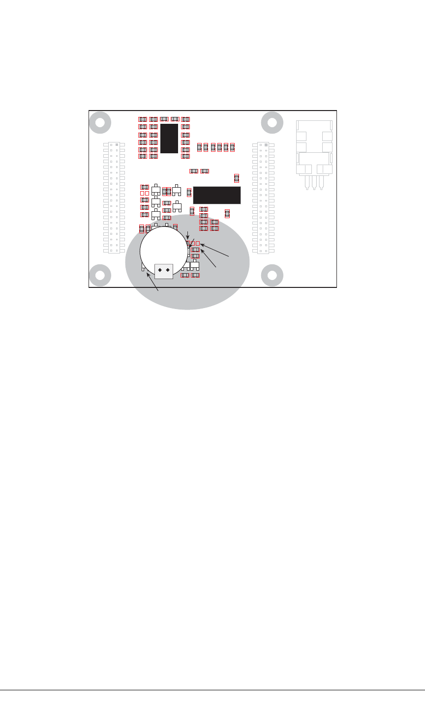
HV3 can also be reconfigured as a sinking output. To do so, remove the 0 Ω surface-
mounted resistor R56, and solder on a 0 Ω surface-mounted resistor or jumper wire at
R55. If you plan to drive inductive loads, add a diode at D21. Figure 8 shows the location
of these components.
Figure 8. Changing HV3 to a Sinking Output
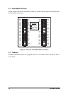
3.2.3 Bidirectional I/O
The Jackrabbit has 14 CMOS-level bidirectional I/O: PA0–PA7, PD0, PD3, PD6–PD7,
and PE4–PE5. The BL1820, which does not have RS-485, has one additional bidirectional
I/O, PD5.
J5
GND
PA0
PA2
PA4
PA6
GND
PB0
PB2
PB4
PB6
WDO
GND
PE6
PE4
PE2
PE0
HV0
HV2
K
GND
VCC
PA1
PA3
PA5
PA7
GND
PB1
PB3
PB5
PB7
PCLK
PE7
PE5
PE3
PE1
GND
HV1
HV3
+RAW
VCC
GND
RXC
TXC
PC1
PC3
PC5
PC7
AGND
DA1
PD1
PD3
PD5
PD7
GND
485+
VCC
SM1
STAT
VBAT
GND
VCC
RXB
TXB
PC0
PC2
PC4
PC6
AD0
DA0
PD0
PD2
PD4
PD6
GND
485
VCC
SM0
IOBEN
GND
/RST
J4
Battery
R55
R56
D21
C27
D24


