User’s Manual 33
3.7 Memory
3.7.1 SRAM
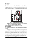
The Jackrabbit is designed to accept 32K to 512K of SRAM packaged in an SOIC case.
Standard Jackrabbit models come with 128K of SRAM. A factory-installed option for 512K
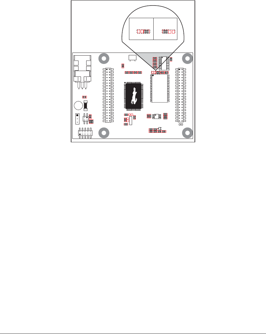
of SRAM is available. Figure 14 shows the locations and the jumper settings for the jump-
ers at JP1 used to set the SRAM size. The “jumpers” are 0 Ω surface-mounted resistors.
Figure 14. Jackrabbit Jumper Settings for SRAM Size
NOTE: For ordering or other information involving the factory-installed 512K SRAM
option, call your Rabbit sales representative or distributor.
No 0 Ω surface-mounted resistors are installed at JP1 for 32K SRAM.
3.7.2 Flash EPROM
The Jackrabbit is also designed to accept 128K to 512K of flash EPROM packaged in a
TSOP case.
NOTE: Rabbit recommends that any customer applications should not be constrained by
the sector size of the flash memory since it may be necessary to change the sector size
in the future.
A Flash Memory Bank Select jumper configuration option exists at JP3 with 0 Ω surface-
mounted resistors for Jackrabbit boards labeled 175-0255. This option, used in conjunc-
tion with some configuration macros, allows Dynamic C to compile two different co-resi-
dent programs for the upper and lower halves of the 256K flash in such a way that both
programs start at logical address 0000. This is useful for applications that require a resi-
dent download manager and a separate downloaded program. See Technical Note 218,
Implementing a Serial Download Manager for a 256K Flash, for details.
U4
1
2
3
JP1
1
2
3
128K
JP1
512K
SRAM
JP1
VINGNDGND
RESET
JACKRABBIT
Z-World, Inc.
GND
PA0
PA2
PA4
PA6
GND
PB0
PB2
PB4
PB6
WDO
GND
PE6
PE4
PE2
PE0
HV0
HV2
K
GND
VCC
PA1
PA3
PA5
PA7
GND
PB1
PB3
PB5
PB7
PCLK
PE7
PE5
PE3
PE1
GND
HV1
HV3
+RAW
VCC
GND
RXC
TXC
PC1
PC3
PC5
PC7
AGND
DA1
PD1
PD3
PD5
PD7
GND
485+
VCC
SM1
STAT
VBAT
GND
VCC
RXB
TXB
PC0
PC2
PC4
PC6
AD0
DA0
PD0
PD2
PD4
PD6
GND
485
VCC
SM0
IOBEN
GND
/RST
J5
U6
U5
U3
J4
U1
J1
J2
J3
Y3
SRAM
RS-232
RS-485


