


76 Jackrabbit (BL1800)
B.3.2 Prototyping Board
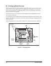
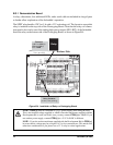
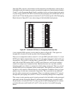
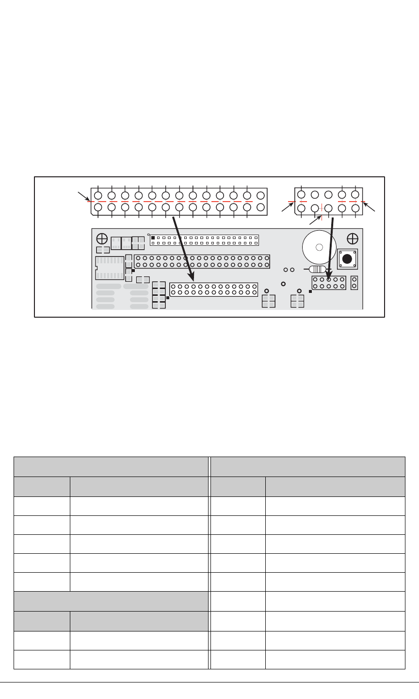
To maximize the availability of Jackrabbit resources, the demonstration hardware (LEDs,
switches, potentiometer, buzzer) on the Prototyping Board may be disconnected. This is
done by cutting the traces seen between and within the silk-screen outline of headers JP1
and JP2 on the Prototyping Board. Figure B-6 shows the 16 places where cuts should be
made. An exacto knife or high-speed precision grinder tool like a Dremel
®
tool would
work nicely to cut the traces. Alternatively, if safety is a major concern, a small standard
screwdriver may be carefully and forcefully used to wipe through the PCB traces.
Figure B-6. Where to Cut Traces to Permanently Disable
Demonstration Hardware on Prototyping Board
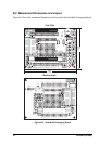
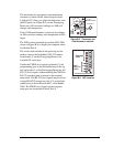
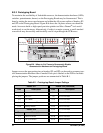
Jumpers across the appropriate pins on headers JP1 and JP2 can be used to reconnect spe-
cific demonstration hardware later if needed. Each pin is labeled on the PCB to facilitate
placing the jumpers. The jumper positions are summarized in Table B-1.
Table B-1. Prototyping Board Jumper Settings
Header JP1 Header JP2 (continued)
Pins Description Pins Description
1–2 Buzzer 5–6 PA2 to LED DS3
3–5 K to +5 V 7–8 PA3 to LED DS4
5–6 K to +RAW 9–10 PA4 to LED DS5
7–8 Potentiometer or Thermistor 11–12 PA5 to LED DS6
9–10 Interrupt Enable 13–14 PA6 to LED DS7
Header JP2 15–16 PA7 to LED DS8
Pins Description 17–18 PB2 to switch S1
1–2 PA0 to LED DS1 19–20 PB3 to switch S2
3–4 PA1 to LED DS2 21–22 PB4 to switch S3
Cut all gray
traces shown
Cut
Cut
Cut
Cut
Buzzer
Top Side
J2
J3
JP1
JP2
1
2
3
R3
R1
LS1
RT1
GND
PA6
PA4
PA2
PA0
PA7
PA5
PA3
PA1
VCC
GND
PE2
PE4
PE6
PE0
HV0
HV2
K
GND
PB5
PB4
PB3
PB2
PA7
PA6
PA5
PA4
PA3
PA2
PA1
PA0
GND
WDO
PB6
PB4
PB2
PB0
GND
VCC
+RAW
HV3
HV1
GND
PE1
PE3
PE5
PE7
PCLK
PB7
PB5
PB3
PB1
GND
BZR
VCC
K
AD0
PE4
POT
HV0
+RAW
DS5
DS4
DS3
DS2
DS1
DS6
DS7
DS8
S1
S2
S3
S4
GND
COIL(+)
COIL(-)
PD0
GND
AD0
+