


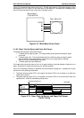
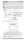
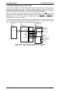
2.1.2.6 Bias Voltages and Laser Drive Timing
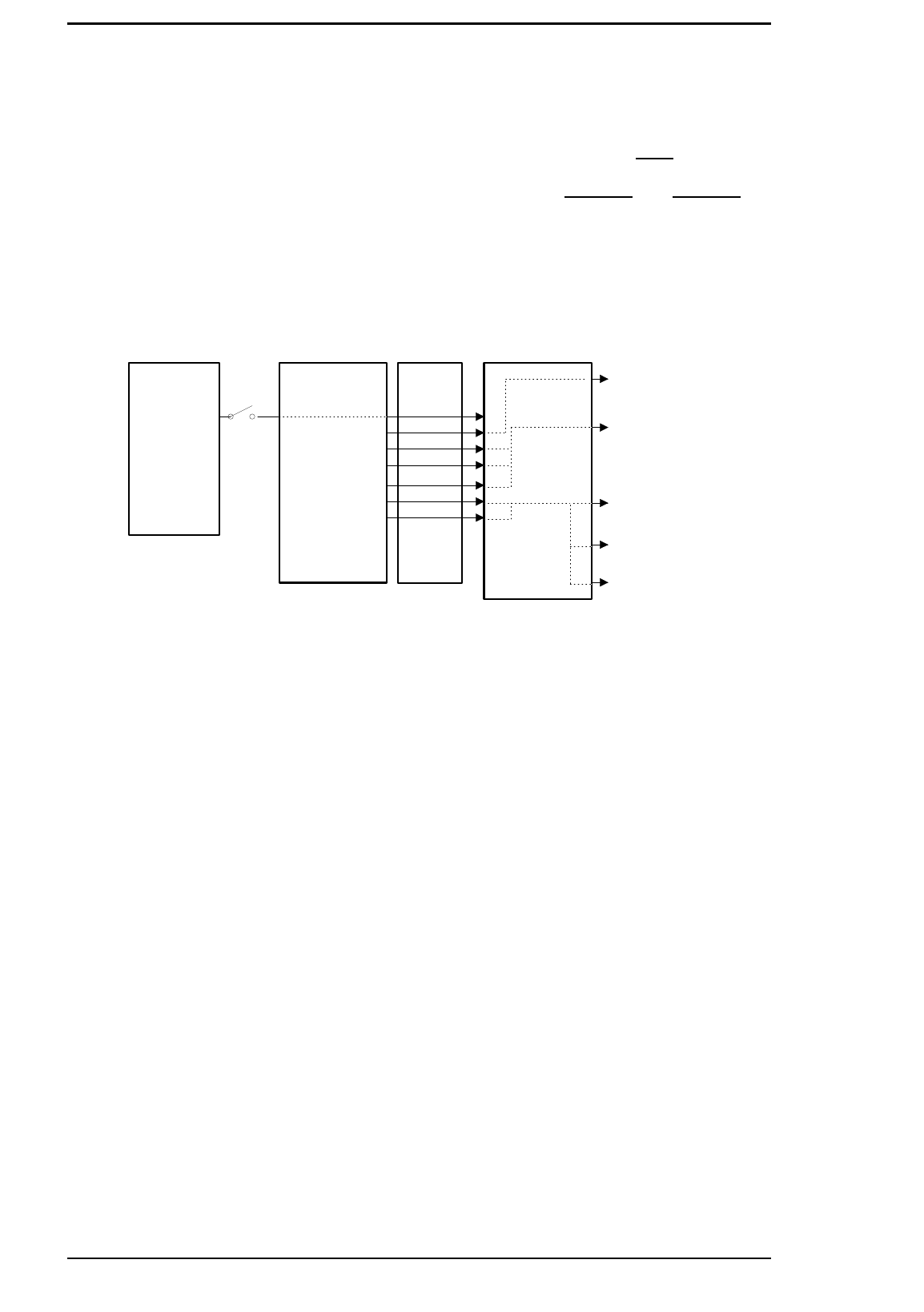
Figure 2-20 is a diagram of the drum charge bias voltage, image transfer bias voltage, and the
developing bias voltage control circuit. These bias voltages are generated from the +24 VDC from
the high-voltage supply board (PWB-F). If the printer detects a case-open condition, the interlock
switch is set to off, which cuts the +24 VDC, which, in turn, cuts the bias voltages.
These bias voltages are controlled by the main board (C169 MAIN-B). The
HV-T signal is the
image transfer bias voltage control. While this signal is LOW, the image transfer electrode comb is
charged to from +3 to +6K VDC by the high-voltage supply circuit.
HV SEL1 and HV SEL2 are
image transfer bias level control signals.
The HVB signal is the digital signal for developing bias voltage control. This signal controls the bias
on/off. The BIAS MON signal controls the bias voltage level (–300 V to –375K VDC) using pulse
data. The image density is controlled by the developing bias voltage level.
+24 VDC
Interlock
SW
Power Supply
Board
(PWB-E)
+24 VDC
HV-C
HV-T
HV SEL1
Image Transfer
Bias
3K to 6 K VDC
Developing
Bias
-270 to -370 VDC
Drum Charge
-2.0 K VDC
Main
Board
(C169 MAIN-B)
High Voltage Supply
Board
(PWB-F)
Doctor Toner Blade
Bias -500 VDC
HV SEL2
HV B
BIAS MON
Seal Bias
-250 VDC
PWB-S
Figure 2-20. High-Voltage Supply Block Diagram
Operating Principles EPL-5500 Service Manual
2-14 Rev. B