


C141-E116-01EN5 - 100
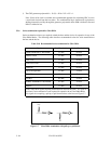
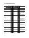
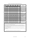
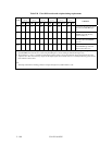
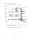
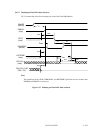
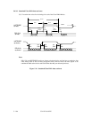
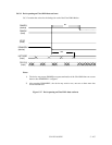
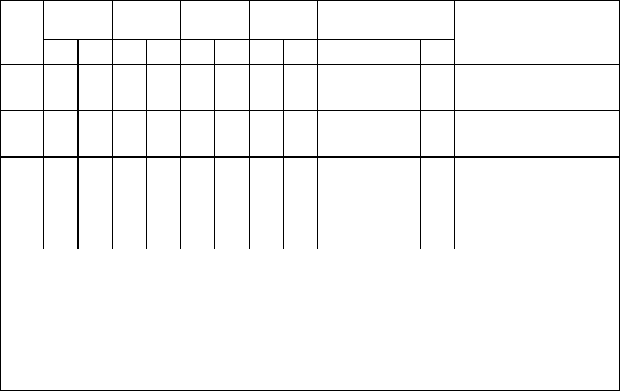
Table 5.20 Ultra DMA sender and recipient timing requirements
MODE 0
(in ns)
MODE 1
(in ns)
MODE 2
(in ns)
MODE 3
(in ns)
MODE 4
(in ns)
MODE 5
(in ns)
NAME
MIN MAX MIN MAX MIN MAX MIN MAX MIN MAX MIN MAX
COMMENT
t
DSIC
14.7 9.7 6.8 6.8 4.8 2.3 Recipient IC data setup time (from
data valid until STROBE edge)
(*1)
t
DHIC
4.8 4.8 4.8 4.8 4.8 2.8 Recipient IC data hold time (from
STROBE edge until data may
become invalid) (*1)
t
DVSIC
72.9 50.9 33.9 22.6 9.5 6 Sender IC data valid setup time
(from data valid until STROBE
edge) (*2)
t
DVHIC
9 9 9 9 9 6 Sender IC data valid hold time
(from STROBE edge until data
may become invalid) (*2)
*1: The correct data value shall be captured by the recipient given input data with a slew rate of 0.4 V/ns rising and falling and the
input STROBE with a slew rate of 0.4 V/ns rising and falling at t
DSIC
and t
DHIC
timing (as measured through 1.5V).
*2: The parameters t
DVSIC
and t
DVHIC
shall be met for lumped capacitive loads of 15 and 40 pf at the IC where all signals have the same
capacitive load value. Noise that may couple onto the output signals from external sources in a normally functioning system has not
been included in these values.
Note:
All timing measurement switching points (low to high and high to low) shall be taken at 1.5V.