


C141-E116-01EN 5 - 7
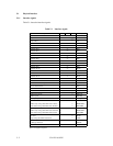
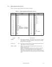
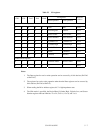
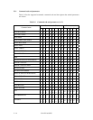
Table 5.3 I/O registers
I/O registers
Read operation Write operation
Command block registers
10000Data Data X'1F0'
10001Error RegisterFeatures X'1F1'
10010Sector CountSector CountX'1F2'
10011Sector NumberSector NumberX'1F3'
10100Cylinder LowCylinder LowX'1F4'
10101Cylinder HighCylinder HighX'1F5'
10110Device/HeadDevice/HeadX'1F6'
10111Status Command X'1F7'
1 1 X X X (Invalid) (Invalid) —
Control block registers
01110Alternate StatusDevice ControlX'3F6'
01111— — X'3F7'
Notes:
1. The Data register for read or write operation can be accessed by 16 bit data bus (DATA0
to DATA15).
2. The registers for read or write operation other than the Data registers can be accessed by
8 bit data bus (DATA0 to DATA7).
3. When reading the Drive Address register, bit 7 is high-impedance state.
4. The LBA mode is specified, the Device/Head, Cylinder High, Cylinder Low, and Sector
Number registers indicate LBA bits 27 to 24, 23 to 16, 15 to 8, and 7 to 0.
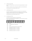
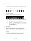
Host I/O
address
DA0DA1DA2CS1–CS0–