


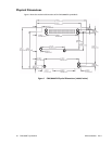


BDM-610000050 Rev A Appendix A: Hardware Reference 81
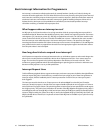
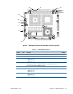
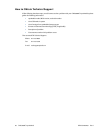
Figure 6 CMX58886CX Jumper and Solder Blob Locations (top side)
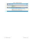
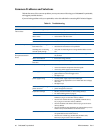
Table 57 CMX58886CX Jumpers
Jumper Pins Function Default
JP1 2 Enable/disable 120 Ω series termination to COM1 (CN7) in RS-422/485 modes open
JP2 2 Enable/disable 120 Ω series termination to COM2 (CN8) in RS-422/485 modes open
JP4 3 Select power for the ATA/IDE Disk Chip
pins 1–2: +5 V
pins 2–3: +3.3 V
pins 2–3
JP5 2 Install to load the default BIOS settings (for more information, refer to the
following section of the manual: System Recovery—page 75). Note that the
multi-color LED will be red if JP5 is installed.
open
JP6 2Reserved open
JP8 3 Select power for the flat panel electronics
pins 1–2: +3.3 V
pins 2–3: +5 V
pins 1–2
JP9 3 Select power for flat panel backlight
pins 1–2: +12 V
pins 2–3: +5 V
pins 2–3
JP9
JP8
JP2
B2
B1
JP4
B7
B3
JP1
JP6
JP5