


EM78P221/2N
8-Bit Microcontroller with OTP ROM
Product Specification (V1.0) 10.19.2007 • 19
(This specification is subject to change without further notice)
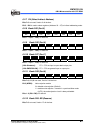
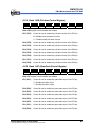
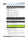
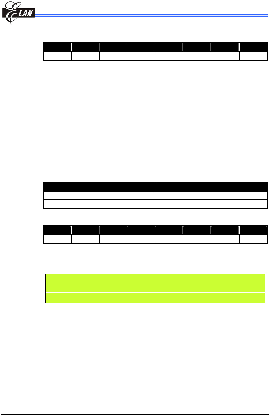
6.2.26 Bank 2-R7 (HSCR2: High Sink Control Register for Port 6)
Bit 7 Bit 6 Bit 5 Bit 4 Bit 3 Bit 2 Bit 1 Bit 0
HS67 HS66 HS65 HS64 HS63 HS62 HS61 HS60
[With Simulator]: function nonexistent
[With EM78P221/2N]: General I/O pins.
Bit 7 (HS67): Output High Sink Current Select for P67
Bit 6 (HS66): Output High Sink Current Select for P66
Bit 5 (HS65): Output High Sink Current Select for P65
Bit 4 (HS64): Output High Sink Current Select for P64
Bit 3 (HS63): Output High Sink Current Select for P63
Bit 2 (HS62): Output High Sink Current Select for P62
Bit 1 (HS61): Output High Sink Current Select for P61
Bit 0 (HS60): Output High Sink Current Select for P60
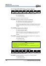
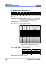
HDxx VDD = 5V, Sink Current
0 18 mA (in 0.1VDD)
1 75 mA (in 0.3VDD)
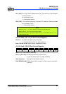
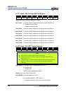
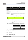
6.2.27 Bank 2-R8 (Operating Mode Control Register)
Bit 7 Bit 6 Bit 5 Bit 4 Bit 3 Bit 2 Bit 1 Bit 0
0 1 1 0 0 0 0 0
Bits 7, 4~0: not used, fixed to "0" all the time.
Bits 6~5: not used, fixed to "1" all the time.
NOTE
■ If user wants the MCU to work normally, user must set Bit 6 and Bit 5 of the R8
register to “1” and clear Bit 4 of R8 register to “0”.
6.2.28 Bank 2-R9~RF (Reserve)
Bits 7~0: not used, fixed to "0" all the time
6.2.29 Bank 3-R5 (Timer Clock/Counter)
Incremented by an external signal edge through the TCC pin, or by the instruction
cycle clock.
External signal of TCC trigger pulse width must be greater than one instruction.
The signals to increase the counter are determined by Bit 4 and Bit 5 of the CONT
register.
Writable and readable as any other registers.