


EM78P221/2N
8-Bit Microcontroller with OTP ROM
Product Specification (V1.0) 10.19.2007 • 23
(This specification is subject to change without further notice)
8-bit CounterWDT
Prescaler8 to 1 MUX
WDT Time out
WDTE (Bank 1-RE)
TCC Pin
MUX
CLK (Fosc)
8-bit Counter
8 to 1 MUX
TE (CONT)
Data Bus
TCC overflow
Interrupt
TS (CONT)
TCC (R1)
0
1
PSW2~0
(Bank 1-RE)
Prescaler
PSR2~0
(CONT)
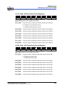
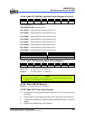
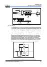
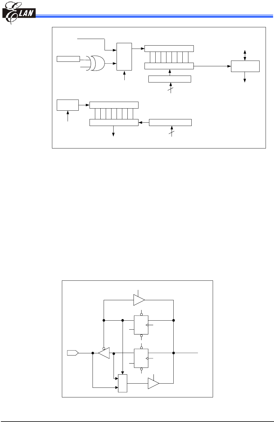
Fig. 6-2 TCC and WDT Block Diagram
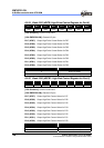
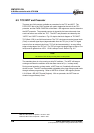
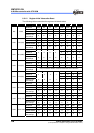
6.4 I/O Ports
The I/O registers (Port 5, Port 6, Port 7, and Port 8) are bidirectional tri-state I/O ports.
The Pull-high, Pull-down, and Open-drain functions can be set internally by Bank 1-RB,
Bank 1-RC, and Bank 1-RD respectively. The High Drive, and High Sink functions can
be set internally by Bank 2-R5, Bank 2-R6, and Bank 2-R7 respectively. Port 6 features
an input status change interrupt (or wake-up) function. Most I/O pin can be defined as
"input" or "output" pin by the I/O control registers (P52, P53 are only used as output
pins). The I/O registers and I/O control registers are both readable and writable.
However, the initial states of these I/O ports (Port 5, Port 6, Port 7 and Port 8) are
unknown input (high impedance). Then, if the I/O pin is pulled to a level at external
circuit, the pin must induce a voltage. Hence, user must take into consideration
whether the induced voltage causes a wrong action in the system. The I/O interface
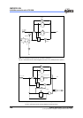
circuits for Port 5, Port 6, Port 7, and Port 8 are illustrated in Figures 6-3, 6-4, & 6-5
respectively. Port 6 with Input Change Interrupt/Wake-up is shown in Fig. 6-6.
M
U
X
PORT
PCWR
PDWR
IOD
PDRD
0
1
PCRD
D
D
Q
Q
Q
Q
_
_
C
L
C
L
P
R
CLK
CLK
P
R
Note: Pull-high and Open-drain are not shown in the figure.
Fig. 6-3 I/O Port and I/O Control Register Circuit for Port 5 , Port 7 and Port 8