Networking Silicon — 82540EP
Datasheet 9
3.0 Signal Descriptions
Note: The targeted signal names are subject to change without notice. Verify with your local Intel sales
office that you have the latest information before finalizing a design.
3.1 Signal Type Definitions
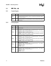
The signals of the 82540EP controller are electrically defined as follows:
3.2 PCI Bus Interface
When the Reset signal (RST#) is asserted, the 82540EP will not drive any PCI output or bi-
directional pins except the Power Management Event signal (PME#).
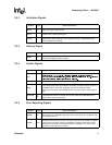
3.2.1 PCI Address, Data and Control Signals
Name Definition
I Input. Standard input only digital signal.
O
Output. Standard output only digital signal.
TS
Tri-state. Bi-directional three-state digital input/output signal.
STS
Sustained Tri-state. Sustained digital three-state signal driven by one agent at a time.
An agent driving the STS pin low must actively drive it high for at least one clock before letting it
float. The next agent of the signal cannot drive the pin earlier than one clock after it has been
released by the previous agent.
OD
Open Drain. Wired-OR with other agents.
The signaling agent asserts the OD signal, but the signal is returned to the inactive state by a
weak pull-up resistor. The pull-up resistor may require two or three clock periods to fully restore
the signal to the de-asserted state.
A
Analog. PHY analog data signal.
P
Power. Power connection, voltage reference, or other reference connection.
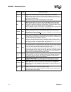
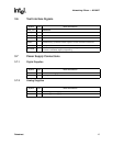
Symbol Type Name and Function
AD[31:0]
TS
Address and Data.
The address phase is the clock cycle when the Frame signal (FRAME#) is asserted
low. During the address phase AD[31:0] contain a physical address (32 bits). For I/O,
this is a byte address, and for configuration and memory, a DWORD address. The
82540EP device uses little endian byte ordering.
During data phases, AD[7:0] contain the least significant byte (LSB) and AD[31:24]
contain the most significant byte (MSB).


