82540EP — Networking Silicon
10 Datasheet
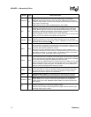
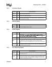
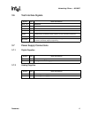
CBE[3:0]#
TS
Bus Command and Byte Enables. Bus command and byte enable signals are
multiplexed on the same PCI pins. During the address phase of a transaction,
CBE[3:0]# define the bus command. In the data phase, CBE[3:0]# are used as byte
enables. The byte enables are valid for the entire data phase and determine which byte
lanes contain meaningful data.
CBE0# applies to byte 0 (LSB) and CBE3# applies to byte 3 (MSB).
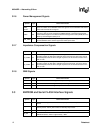
PA R TS
Parity. The Parity signal is issued to implement even parity across AD[31:0] and
CBE[3:0]#. PAR is stable and valid one clock after the address phase. During data
phases, PAR is stable and valid one clock after either IRDY# is asserted on a write
transaction or TRDY# is asserted after a read transaction. Once PAR is valid, it remains
valid until one clock after the completion of the current data phase.
When the 82540EP controller is a bus master, it drives PAR for address and write data
phases, and as a slave device, drives PAR for read data phases.
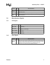
FRAME# STS
Cycle Frame. 82540EP device to indicate the
beginning and length of an access and indicate the beginning of a bus transaction.
While FRAME# is asserted, data transfers continue. FRAME# is de-asserted when the
transaction is in the final data phas
IRDY# STS
Initiator Ready. Initiator Ready indicates the ability of the 82540EP controller (as bus
master device) to complete the current data phase of the transaction. IRDY# is used in
conjunction with the Target Ready signal (TRDY#). The data phase is completed on any
clock when both IRDY# and TRDY# are asserted.
During the write cycle, IRDY# indicates that valid data is present on AD[31:0]. For a
read cycle, it indicates the master is ready to accept data. Wait cycles are inserted until
both IRDY# and TRDY# are asserted together. The 82540EP controller drives IRDY#
when acting as a master and samples it when acting as a slave.
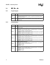
TRDY# STS
Target Ready. The Target Ready signal indicates the ability of the 82540EP controller
(as a selected device) to complete the current data phase of the transaction. TRDY# is
used in conjunction with the Initiator Ready signal (IRDY#). A data phase is completed
on any clock when both TRDY# and IRDY# are sampled asserted.
During a read cycle, TRDY# indicates that valid data is present on AD[31:0]. For a write
cycle, it indicates the target is ready to accept data. Wait cycles are inserted until both
IRDY# and TRDY# are asserted together. The 82540EP device drives TRDY# when
acting as a slave and samples it when acting as a master.
STOP# STS
Stop. The Stop signal indicates the current target is requesting the master to stop the
current transaction. As a slave, the 82540EP controller drives STOP# to request the
bus master to stop the transaction. As a master, the 82540EP controller receives
STOP# from the slave to stop the current transaction.
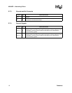
IDSEL# I
Initialization Device Select. The Initialization Device Select signal is used by the
82540EP as a chip select signal during configuration read and write transactions.
DEVSEL# STS
Device Select. When the Device Select signal is actively driven by the 82540EP, it
signals notifies the bus master that it has decoded its address as the target of the
current access. As an input, DEVSEL# indicates whether any device on the bus has
been selected.
VIO P
VIO. The VIO signal is a voltage reference for the PCI interface (3.3 V or 5 V PCI
signaling environment). It is used as the clamping voltage.
Note: An external resistor is required between the voltage reference and the VIO pin.
The target resistor value is 100 K
Ω
Symbol Type Name and Function


