Networking Silicon — 82540EP
Datasheet 13
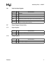
3.4 Miscellaneous Signals
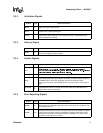
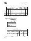
3.4.1 LED Signals
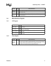
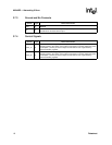
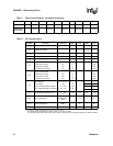
3.4.2 Other Signals
FL_CE# O FLASH Chip Enable Output. Used to enable FLASH device.
FL_SCK O
FLASH Serial Clock Output. The clock rate of the serial FLASH interface is
approximately 1 MHz.
FL_SI O
FLASH Serial Data Input. This pin is an output to the memory device.
FL_SO I
FLASH Serial Data Output. This pin is an input from the FLASH memory. It has an
internal pullup device.
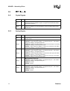
Symbol Type Name and Function
Symbol Type Name and Function
LED0 / LINK# O
LED0 / LINK Up. Programmable LED indication. Defaults to indicate link
connectivity.
LED1 / ACT# O
LED1 / Activity. Programmable LED indication. Defaults to flash to indicate
transmit or receive activity.
LED2 / LINK100# O
LED2 / LINK 100. Programmable LED indication. Defaults to indicate link at
100 Mbps.
LED3 / LINK1000# O
LED3 / LINK 1000. Programmable LED indication. Defaults to indicate link at
1000 Mbps.
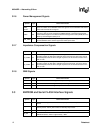
Symbol Type Name and Function
SDP[7:6]
SDP[1:0]
TS
Software Defined Pin. The Software Defined Pins are reserved and programmable
with respect to input and output capability. These default to input signals upon power-up
but may be configured differently by the EEPROM. The upper four bits may be mapped
to the General Purpose Interrupt bits if they are configured as input signals.
Note: SDP5 is not included in the group of Software Defined Pins.


