


82555 — Networking Silicon
8
Datasheet
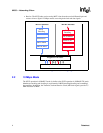
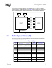
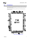
Pin allocation is based on a 100-lead quad flat package. All pin locations are based on printed
circuit board layout and other design constraints.
3.1 Pin Types
3.2 Clock Pins
3.3 Twisted Pair Ethernet (TPE) Pins
3.4 Media Independent Interface (MII) Pins
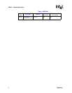
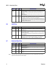
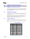
Pin Type Description
I This type of pin is an input pin to the 82555.
O This type of pin is an output pin from the 82555.
I/O This type of pin is both an input and output pin for the 82555.
B This pin is used as a bias pin. The bias pin is either pulled up or down with a resistor. The bias pin
may also be used as an external voltage reference.
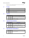
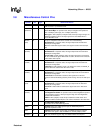
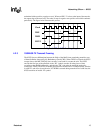
Symbol Pin Type Name and Function
X1 56 I
Crystal Input One.
X1 and X2 can be driven by an external 25 MHz crystal.
Otherwise, X1 may be driven by an external MOS level 25 MHz oscillator
when X2 is left floating. (The crystal should have a tolerance of 50 PPM or
better.)
X2 55 O
Crystal Output Two.
X1 and X2 can be driven by an external 25 MHz
crystal. Otherwise, X1 may be driven by an external MOS level 25 MHz
oscillator when this pin is left floating.
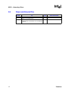
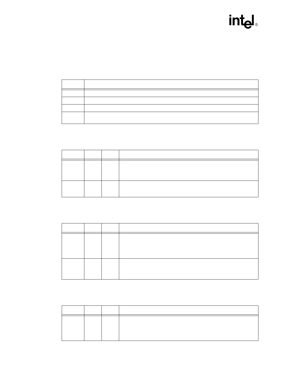
Symbol Pin Type Name and Function
TDP
TDN
47
48
O
Transmit Differential Pair.
These pins send the serial bitstream for
transmission on an unshielded twisted pair (UTP) cable. The current-driven
differential driver can be two-level (10BASE-T or Manchester) or three-level
(100BASE-TX or MLT-3) signals depending on the operating mode. These
signals interface directly with an isolation transformer.
RDP
RDN
33
34
I
Receive Differential Pair.
These pins receive the serial bitstream from the
isolation transformer. The bitstream can be two-level (10BASE-T or
manchester) or three-level (100BASE-TX or MLT-3) signals depending on the
operating mode.
Symbol Pin Type Name and Function
RXD3
RXD2
RXD1
RXD0
97
96
95
92
O
Receive Data.
In 100 Mbps and 10 Mbps mode, data is transferred across
these four lines one nibble at a time.