


Board Manual 85
IQ80310 and IQ80321 Comparisons A
This appendix provides a brief description for differences between IQ80321 and IQ80310. Please also
refer to application note: Migrating from the Intel
®
80310 I/O Processor Chipset to the Intel
®
80321
I/O Processor Application Note 273562.
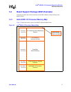
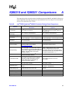
Table 90. Intel
®
IQ80310 and Intel
®
IQ80321 Evaluation Platform Board Comparisons
Features
Intel
®
IQ80321 Evaluation Platform Board
“Worchester”
Intel
®
IQ80310 Evaluation Platform Board
“Cyclone”
I/O Processor Intel
®
80321 I/O processor
Intel
®
80310 I/O processor chipset -Consists of
Intel
®
80200 processor and Intel
®
80312 I/O
companion chip
Core/Microprocessor
Technology
Intel
®
XScale™ microarchitecture Intel
®
XScale™ microarchitecture
Memory Technology PC1600 DDR SDRAM (100 MHz Clock) PC100 SDRAM (100 MHz Clock)
Form Factor
Extended PC board that attaches to a
PC/Server/Backplane – One PCI-X Expansion Slot
Extended PC board that attaches to a
PC/Server/Backplane – Two PCI Expansion Slots
PC/Server/Backplane
Connection
PCI-X 133-MHz/64-Bits or
PCI 66 MHz/64 Bits
PCI 66 MHz/64 Bits
Expansion Card Slot One PCI-X 133-MHz/64-bit Two PCI 66 MHz/64 bits
PCI/PCI-X Bridge
IBM PCI-X Bridge
Reference: IBM 133 PCI-X Bridge
http://www.chips.ibm.com/
Integrated PCI bridge in 80312.
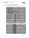
Interrupt Routing
External interrupts are routed through the XINT
pins on the 80321. They include INTA, INTB form
PCI-X expansion slot, INTA from 82544 GBE, and
UART interrupt – Steering and Status registers are
in 80321 – see
Intel
®
80321 I/O Processor
Developer’s Manual
UART1, UART2, External Timer, and Secondary
INTD are multiplexed in the CPLD and
connected to 80312 external interrupt (XINT3).
Secondary PCI INTA, B, C are straight through
connection to 80312 XINT0, 1, 2.
Timers
Internal to 80321 – Refer to
Intel
®
80321 I/O
Processor Developer’s Manual
In CPLD
Local/Peripheral Bus
32-bit/33-100MHz multiplexed bus with six
chip-enables, Synch/Asynchronous (IQ80321
operates in 33 MHz Asynchronous mode) –
Refer to PBI section in
Intel
®
80321 I/O
Processor Developer’s Manual
8-bit multiplexed Flash-bus with two
chip-enables
Flash Memory
16-bit, 8 MB accessed through Peripheral Bus
with chip-enable 0 (PCE0)
8-bit, 8 MB accessed trough Flash-Bank 1 with
chip-enable 1 (RCE1)
Serial Debug Port
One UART on the Peripheral bus – 16C550
device
Two UART on the Flash bank with some logic in
the CPLD – 16C550 device
Network Debug Port Intel® 82544 GbE on the PCI-X bus
Intel® 82559 PRO100 device on the secondary
PCI Bus
Rotary Switch Same Same
LED HEX Display Same Same
JTAG 20-PIN ARM Compliant
Logic Analyzer Connection