


56K V.92 Data, Fax, and Voice Chipset
122 Intel Confidential Programmer’s Guide
In FIFO mode, the modem keeps track of the character in which an error has occurred and does not report the error to the DTE
until the associated character gets to the top of the stack.
Note: In FIFO mode, the DTE must write a data byte in the RX FIFO by the loopback mode to write to LSR2–LSR4. LSR0 and LSR7
cannot be written to in FIFO mode.
10.1.4 Modem Control Register (MCR)
Bit 7
Error in RCVR FIFO–In 16C450 emulation mode, this bit is always a “0”.
In FIFO mode, this bit is set to “1” by the DCE whenever at least one parity error, framing error, or break indi-
cation has occurred in the RCVR FIFO. This bit is cleared when the DTE reads the LSR register and there
are no subsequent FIFO errors.
Bit 6
TEMT (Transmitter Empty)–This bit is set to “1” by the DCE whenever the THR (Transmit Holding register)
and transmitter shift register are empty. This bit is automatically reset to “0” by the DCE whenever the host
writes a byte to the THR.
In FIFO mode, this bit is set to “1” whenever the transmitter FIFO and shift register are both empty.
Bit 5
THRE (Transmitter Holding Register Empty)–This bit is set to “1” whenever the THR (Transmit Holding
register) is empty. This bit is set to “0” whenever the host writes data into the THR. Additionally, if the
THREIE (Transmitter Holding Register Empty Interrupt Enable) is set to “1”, the modem causes an interrupt
to the host whenever THRE goes to “1”.
In FIFO mode, this bit is set to ‘1’ whenever the XMIT FIFO is empty. This bit is then reset to ‘0’ when at least
one byte is written to the XMIT FIFO.
Bit 4
BI (Break Interrupt)–This bit is set to “1” whenever the received data are spaces (logic 0) for at least 2M +
3 bits (M = start bit + # of data character bits + parity bit + # of stop bits). This bit is reset to ‘0’ whenever the
host reads the LSR register. The modem waits for the valid start bit, before again transferring data to the
FIFO.
When a break occurs in FIFO mode, a single null character is placed in the RVCR FIFO. The BI bit is then
set when the zero character gets to the top of the FIFO stack.
Bit 3
FE (Framing Error)–This bit is set to “1” whenever a valid stop bit (logic 1) has not been detected after the
last data bit or parity bit. This bit is reset to “0” whenever the host reads the LSR register. The UART tries to
resynchronize after a framing error.
In FIFO mode, the modem FE bit is set to “1” whenever the associated framing error character has reached
the top of the stack.
Bit 2
PE (Parity Error)–This bit is set to “1” whenever the received data character does not have the correct even
or odd parity, as selected by the EPS (even parity select) bit [LCR4] and the stick parity bit [LCR 5]. This bit
is reset to “0” whenever the host reads the LSR register.
In FIFO mode, the modem PE bit is set to “1” whenever the associated framing error character has reached
the top of the stack.
Bit 1
OE (Overrun Error)–Not supported.
Bit 0
Data Ready–This bit is set to “1” whenever the modem writes a new received data character into the RBR
(Receiver Buffer register) or FIFO. This bit is reset to “0” whenever the DTE reads the RBR or FIFO.
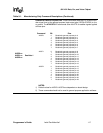
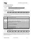
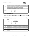
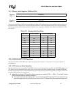
0 0 0 Loop Out 2 Out 1 RTS DTR
Register 4