


56K V.92 Data, Fax, and Voice Chipset
Programmer’s Guide Intel Confidential 123
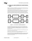
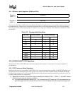
This register controls the DTE-DCE UART interface.
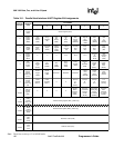
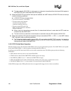
10.1.5 Line Control Register (LCR)
This register specifies the asynchronous data communication exchange format. The modem supports up to 10-bit data characters
(1 start bit + # of data character bits + parity + # of stop bits).
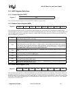
Bit 7:5
Not used–These bits are permanently set to “0”.
Bit 4
Loop Bit–When set to “1”, this bit configures the UART for loopback diagnostic testing. In diagnostic mode,
any data that is written to the THR (Transmit Holding register) is looped back to the RBR (Receiver Buffer
register).
After writing a data byte to the THR register in loopback mode, the DTE must read the RBR register before
writing a new data byte to the THR.
Unlike a real 16C450 UART, the modem signals OUT1*, OUT2*, RTS*, and DTR* are not looped back to the
MSR register.
Bit 3
Out 2–This bit, when set to “1” by the DTE, enables the HINT output pin. When set to “0”, this bit causes the
HINT pin to be in a high-impedance state.
Bit 2
Out 1–This read/write bit is not used for any specific functions.
Bit 1
RTS (Request to Send)–This bit when set to “1”, indicates that the DTE is ready to send data to the
modem.
Bit 0
DTR (Data Terminal Ready)–When set to “1”, this bit indicates that the DTE is read to establish a communi-
cation link.
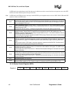
Bit 7
Divisor Latch Access Bit (DLAB) – This bit must be set to “1” to access the divisor latches of the baud rate
generator during a read or write operation. The UART registers 1 and 0 are used for the divisor latches. This
bit must be set to “0” to access the Receiver Buffer register (RBR), the THR (Transmitter Holding register) or
the IER (Interrupt Enable register).
Bit 6
SBRK (Set Break)–This bit is used to send a long-space disconnect message to the remote modem.
The procedure is as follows:
1)After the THRE bit has been set to “1” by the DCE and before setting the SBRK bit, the DTE needs to write
a NULL ($00h) character to the THR.
2)The DTE then sets the SBRK bit after the next time the THRE bit is set by the DCE (a long space is now
being transmitted).
3)To return to normal transmission mode, wait for the TEMT to be equal to “1”, then reset the SBRK bit.
Bit 5
SPAR (Stick Parity)–When this bit is set to “1”, stick parity is enabled. When configured for stick parity
(SPAR = 1), even parity (EPS = 1) with parity enable (PEN = 1), then the parity bit is transmitted and
checked as a logic “0”. When configured for stick parity (SPAR = 1), odd parity (EPS = 0) and parity enable
(PEN = 1) are set to “1”, then the parity bit is transmitted and checked as a logic “1”.
Bit 4
EPS (Even Parity Select)–When even parity select (LCR4) and parity enable (LCR3) are set to “1”, an even
number of logic 1’s are transmitted or checked. When even parity select (LCR4) is a ‘0’ and parity enable
(LCR3) is a “1”, an odd number of logic 1’s are transmitted or checked.
Bit 3
PEN (Parity Enable)–When this bit is set to “1”, a parity bit is generated (transmitted data) or checked
(receive data) between the last data character word bit and stop bit of the serial data.
NOTE: The parity bit is used to produce an even or odd number of 1’s when the data word bits and the parity
bits are summed.
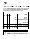
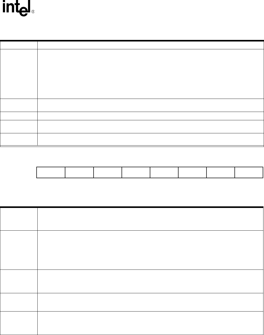
DLAB SBRK SPAR EPS PEN STB WLS1 WLS0
Register 3