Chapter 2 Hardware Overview of the NI 783xR
© National Instruments Corporation 2-21 NI 783xR User Manual
Switch Settings
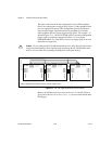
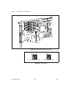
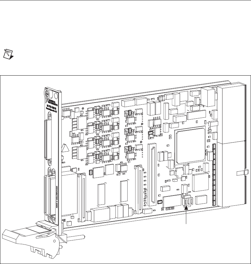
Refer to Figure 2-12 for the location of switches on the NI PXI-783xR and
Figure 2-13 for the location of switches on the NI PCI-783xR. For normal
operation, SW1 is in the OFF position. To prevent a VI stored in flash
memory from loading to the FPGA at power up, move SW1 to the
ON position, as shown in Figure 2-14.
Note SW2 and SW3 are not connected.
Figure 2-12. Switch Location on the NI PXI-783xR
SW1, SW2, SW3


