Chapter 3 Signal Connections
© National Instruments Corporation 3-29 PCI-1200 User Manual
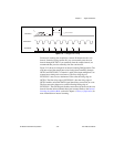
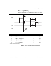
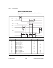
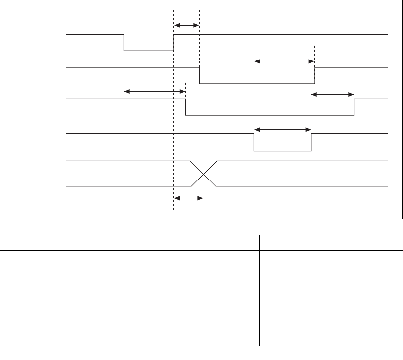
Mode 1 Output Timing
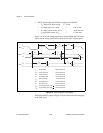
The timing specifications for an output transfer in mode 1 are as follows:
Figure 3-18.
Mode 1 Timing Specifications for Output Transfers
Name Description Minimum Maximum
T1
WRT* = 0 to INTR = 0
— 450
T2
WRT* = 1 to output
— 350
T3
WRT* = 1 to OBF* = 0
— 650
T4
ACK* = 0 to OBF* = 1
— 350
T5
ACK* pulse width
300 —
T6
ACK* = 1 to INTR = 1
— 350
All timing values are in nanoseconds.
WRT*
OBF*
INTR
ACK*
DATA
T1
T2
T3
T4
T5
T6


