Appendix A Specifications
PCI-1200 User Manual A-8 © National Instruments Corporation
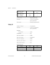
Power-on state ........................................All ports mode 0 input
Protection................................................–0.5 to 5.5 V powered on,
±0.5 V powered off
Data transfers..........................................Interrupts, programmed I/O
Timing I/O
Number of channels................................3 counter/timers
Protection................................................–0.5 to 5.5 V powered on,
±0.5 V powered off
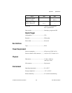
Resolution
Counter/timers.................................16 bits
Compatibility ..........................................TTL
Base clock available ...............................2 MHz
Base clock accuracy................................±50 ppm max
Max source frequency.............................8 MHz
Min source pulse duration ......................125 ns
Min gate pulse duration ..........................50 ns
Digital logic levels
Output low voltage
(I
OUT
= 2.5 mA) — 0.4 V
Output high voltage
(I
OUT
= –40 µA)
(I
OUT
= –2.5 mA)
4.2 V
3.7 V
—
—
Level Min Max
Input low voltage –0.3 V 0.8 V
Input high voltage 2.2 V 5.3 V


