Chapter 4 Theory of Operation
© National Instruments Corporation 4-7 PCI-1200 User Manual
Stanley P. Lipshitz, Journal of the Audio Engineering Society, Vol. 35,
No. 12, Dec. 1987.
The PCI-1200 uses a 12-bit successive-approximation ADC. The
converter’s 12-bit resolution allows it to resolve its input range into 4,095
different steps. The ADC has an input range of ±5 V and 0 to 10 V.
When an A/D conversion is complete, the ADC clocks the result into the
A/D FIFO. The A/D-FIFO is 16 bits wide and 4,096 words deep. This FIFO
serves as a buffer to the ADC. The A/D FIFO can collect up to 4,096 A/D
conversion values before any information is lost, thus allowing software
some extra time to catch up with the hardware. If you store more than 4,096
values in the A/D FIFO before reading from it, an error condition called
A/D FIFO overflow occurs and you lose A/D conversion information.
The ADC output can be interpreted as either straight binary or two’s
complement, depending on which coding scheme you select. Straight
binary is the recommended coding scheme for unipolar input mode. With
this scheme, the ADC data is interpreted as a 12-bit straight binary number
with a range of 0 to +4,095. Two’s complement is the recommended coding
scheme for bipolar input mode. With this scheme, the ADC data is
interpreted as a 12-bit two’s complement number with a range of –2,048 to
+2,047. The ADC output is then sign-extended to 16 bits, causing either a
leading 0 or a leading F (hex) to be added, depending on the coding and the
sign. Thus, data values read from the FIFO are 16-bits wide.
DAQ Operations
This manual uses the phrase data acquisition operation (abbreviated as
DAQ operation) to refer to a sequence of timed A/D conversions. The
PCI-1200 performs DAQ operations in one of three modes: controlled
acquisition mode, freerun acquisition mode, and interval scanning
acquisition mode. The PCI-1200 performs both single-channel and
multichannel scanned data acquisition.
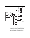
The DAQ timing circuitry consists of various clocks and timing signals that
control the DAQ operation. DAQ timing consists of signals that initiate a
DAQ operation, time the individual A/D conversions, gate the DAQ
operation, and generate scanning clocks. The DAQ operation can be timed
either by the timing circuitry or by externally generated signals. These two
timing modes are software configurable.
DAQ operations are initiated either externally through EXTTRIG or
through software control. The DAQ operation is terminated either
internally by counter A1 of the 82C53 (A) counter/timer circuitry, which


