Chapter 4 Theory of Operation
PCI-1200 User Manual 4-12 © National Instruments Corporation
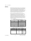
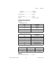
voltage increment corresponding to an LSB change in the digital code
word. For both outputs:
DAC Timing
There are two modes in which you can update the DAC voltages. In
immediate update mode, the DAC output voltage is updated as soon as you
write to the corresponding DAC. In delayed update mode, the DAC output
voltage does not change until a low level is detected either from counter A2
of the timing circuitry or EXTUPDATE*. This mode is useful for
waveform generation. These two modes are software selectable.
Digital I/O
The digital I/O circuitry has an 82C55A integrated circuit. The 82C55A
is a general purpose programmable peripheral interface containing 24
programmable I/O pins. These pins represent the three 8-bit I/O ports
(A, B, and C) of the 82C55A, as well as PA<0..7>, PB<0..7>, and
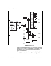
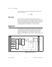
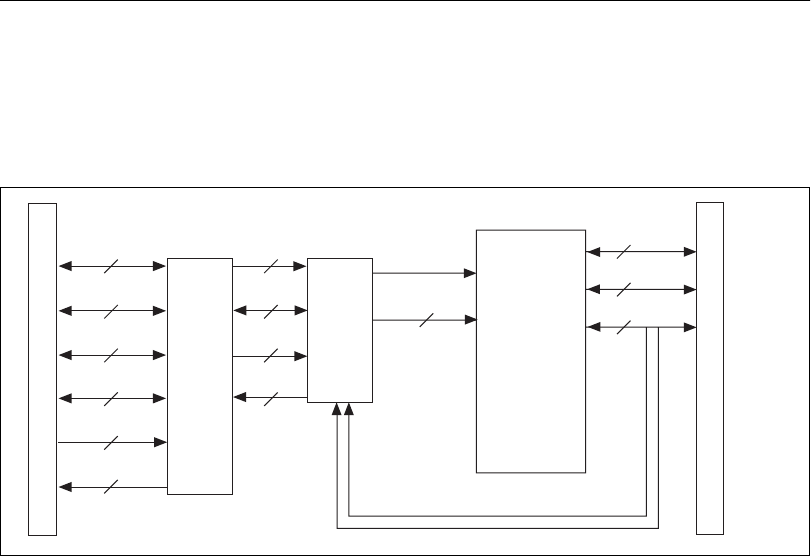
PC<0..7> on the PCI-1200 I/O connector. Figure 4-6 shows the digital I/O
circuitry.
Figure 4-6.
Digital I/O Circuitry
1
LSB
10
V
4095
,
---------------=
82C55A
Programmable
Peripheral
Interface
DIO RD/WRT
DATA<0..7>
PC0
PC3
PC<0..7>
PB<0..7>
PA<0..7>
I/O Connector
2
8
8
8
PCI Bus
Digital
Control
Logic
MITE
PCI
Interface
Chip
Data/Address
Interface Control
Error Reporting
Arbitration
System
Interrupt
1
2
2
2
6
37
Address
Data
Control
Interrupt
1
4
8
5


