Chapter 4 Theory of Operation
PCI-1200 User Manual 4-4 © National Instruments Corporation
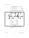
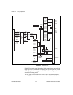
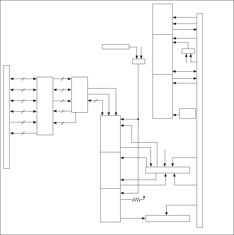
Figure 4-3.
Timing Circuitry
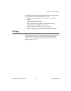
Each 82C53 contains three independent 16-bit counter/timers and one 8-bit
mode register. Each counter has a CLK input pin, a GATE input pin, and an
OUT output pin. You can program all six counter/timers to operate in
several useful timing modes.
The first group of counter/timers is called group A and includes A0, A1,
and A2. You can use these three counters for internal DAQ and DAC
2 MHz
Source
A/D Conversion Logic
1 MHz Source
OUTB0
CLKA0
GATEB0
OUTB0
CLKB1
GATEB1
OUTB2
GATEB2
CLKB2
D/A Conversion Logic
82C53 Counter/Timer
Group A
CTR RD
CTR WRT
Data
8
82C53 Counter/Timer
Group B
OUTB0
OUTB2
GATEB2
CLKB2
GATEB1
Scan
Interval/
General
Purpose
Counter
CLKB1
OUTB1
GATEB0
Timebase
Extension/
General
Purpose
Counter
CLKB0
+5 V
MUX
MUX
EXTUPDATE*
EXTTRIG
EXTCONV*
I/O Connector
CLKA2
OUTA0
Sample
Interval
Counter
CLKA0
GATEA0
CLKA1
Sample
Counter
GATEA1
OUTA1
GATEA2
DAC
Timing
OUTA2
General
Purpose
Counter
OUTB1
OUTB1
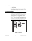
PCI Bus
Digital
Control
Logic
MITE
PCI
Interface
Chip
Data/Address
Interface Control
Error Reporting
Arbitration
System
Interrupt
1
2
2
2
6
37
Address
Data
Control
Interrupt
1
DRQ
1
4
8
5


