


C – 9
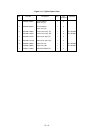
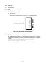
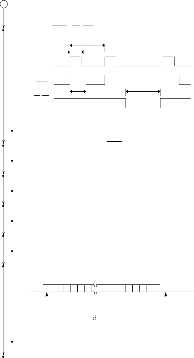
Figure C-3-4
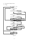
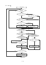
A
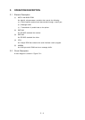
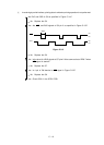
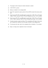
Yes Are ALE, PSEN, RD, WR, signals as specified in Figure C-3-3?
No Replace the Q3.
Yes Are (T1) SELECT and (INTO) BUSY signals low level?
No Check Q501 on the SDDV board.
Yes Are +9V and -9V input to Q1?
No Replace defective component in +9/–9 volt control circuit.
Yes Is pin 1 SSD signal of Q3 High level?
No Replace the Q3.
Yes Is pin 11 SSD of Q1 low level?
No Replace the Q1 or the CN1?
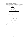
Yes Is the RxD of Q3 as specified in Figure C-3-4?
No Replace the Q2.
Yes Replace the Q3.
542ns
180ns
271ns
542ns
5V
0V
5V
0V
5V
0V
ALE
PSEN
RD/WR
Figure C-3-3
ST bit SP bit
5V
0V
5V
0V
RxD
SSD