


( 12 / 48 )
IMPORTANT
Notes on Differences between Actual MCU and Emulator:
• Emulator operation differs from mask MCU operation, as listed below:
(1) Reset condition
(2) Initial values of internal resource data at power-on
(3) Internal RAM and ROM capacities, etc.
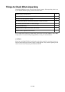
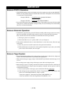
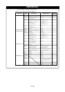
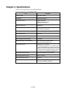
(4) Ports P00 to P57
Of the M306V0T-RPD-E's I/O ports, ports P00 - P57 are connected to the user's target system
through the port emulation circuit inside M306V0T-RPD-E.
Table 1.1 gives the device which uses these ports.
Table 1.1 I/O device used by each of the ports
(5) Writing into pullup control registers 0 and 1 (addresses 03FC16 and 03FD16 respectively)
To write into pullup control registers 0 and 1 (addresses 03FC16 and 03FD16 respectively), it
is necessary to write the word data from address 03FC16. This is an M306V0T-RPD-E
restriction.
(6) Ports P50 - P53
To enable pullup when setting bit 2 (PUR12) of the pullup register 1 to '1' in single chip mode,
be sure to set the bit 2 (PM02) and bit 7 (PM07) of the processor mode register 0 to '0'. This
is an M306V0T-RPD-E restriction.
(7) BCLK output disable
To disable the BCLK output, it is necessary to set the BCLK output disable bit (PM07) of
processor mode register 0 (address 000416) to '1' and to set bit 3 of the port P5 direction register
(address 03EB16) to '0'. This is an M306V0T-RPD-E restriction.
(8) Hold control
When an 'L' level signal is input to the terminal HOLD and the terminal enters the hold state,
in actuality, ports P00 to P52 enter the hold state one half cycle later than the MCU (see Chapter
7, Operation Timing).
(9) A/D converter
A/D converter characteristics differ from actual MCU characteristics because the flexible
cable and other elements are used between the emulation MCU and user’s target.
(10) Status while the program is stopped
In a system using the PC4701, the loop iteration at the address F800016 establishes and
maintains the status during program stop. Also, when debug commands are issued to check
or edit memory data, addresses F800016 to F83FF16 and addresses F600016 to F63FF16 are used
as work area. For this reason, when the CS0 output is enabled in the microprocessor mode,
the CS0 signal is output.
Port
P00-P57
I/O device
M60074-0111FP