


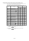
( 32 / 48 )
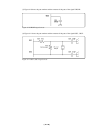
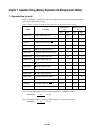
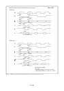
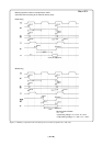
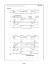
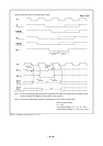
7.2 Separate Bus (with wait), When Accessing to External Memory Area
Table 7.2 and Figure 7.2 show bus timing when using the memory expansion mode and micropro-
cessor mode (with wait, when accessing to the external memory area).
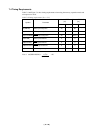
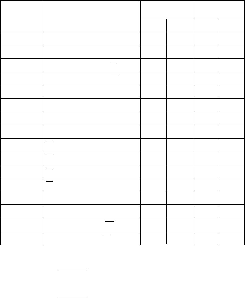
Table 7.2 Memory expansion mode and microprocessor mode (separate bus, with wait)
Note 1. Compute bus timing according to BCLK frequency. Use the below formula.
td(DB-WR) = 10
9
- 40 [ns]
f(BCLK)x2
Note 2. Compute bus timing according to BCLK frequency. Use the below formula.
td(DB-WR) = 10
9
- 55 [ns]
f(BCLK)x2
Address output delay time
Address output hold time (BCLK)
Address output hold time (RD)
Address output hold time (WR)
Chip-select output delay time
Chip-select output hold time (BCLK)
ALE signal output delay time
ALE signal output hold time
RD signal output delay time
RD signal output hold time
WR signal output delay time
WR signal output hold time
Data output delay time (BCLK)
Data output hold time (BCLK)
Data output delay time (WR)
Data output hold time (WR)
Max.
25
-
-
-
25
-
25
-
25
-
25
-
40
-
-
-
Symbol
Min.
-
4
0
0
-
4
-
-4
-
0
-
0
-
4
(Note 1)
0
Parameter
M306V0EEFP
[ns]
td(BCLK-AD)
th(BCLK-AD)
th(RD-AD)
th(WR-AD)
td(BCLK-CS)
th(BCLK-CS)
td(BCLK-ALE)
th(BCLK-ALE)
td(BCLK-RD)
th(BCLK-RD)
td(BCLK-WR)
th(BCLK-WR)
td(BCLK-DB)
th(BCLK-DB)
td(DB-WR)
th(WR-DB)
M306V0T-RPD-E
[ns]
Min.
-
4
-5
-3
-
4
-
-4
-
0
-
0
-
2
(Note 2)
0
Max.
47
-
-
-
36
-
14
-
40
-
40
-
70
-
-
-