( 38 / 48 )
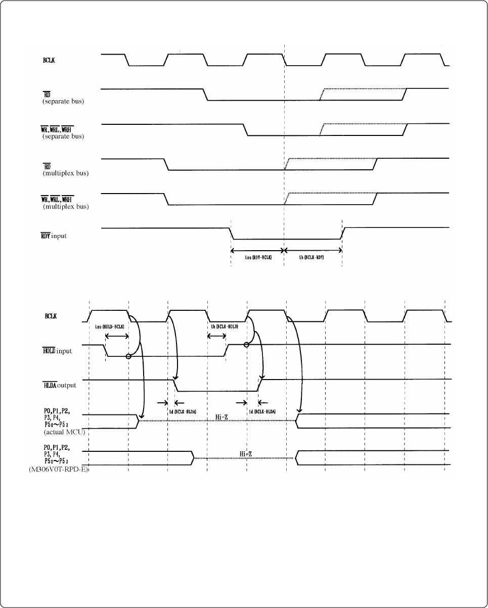
Figure 7.4 Timing requirements (Vcc = 5 V)
Measurement Condition
• VCC = 5 V
• Input timing voltage: VIL = 1.0 V, VIH = 4.0 V
• Output timing voltage: VOL = 2.5 V, VOH = 2.5 V
Vcc = 5 V
Memory expansion mode or microprocessor mode
Note 1. P0
0 to P52 will be high-impedance status regardless of the input level of BYTE pin and ports P40 to P43
function selection bit (PM06) of the processor mode register 0.
Note 2. This product will be high-impedance delaying by 0.5 cycles than an actual MCU.


