


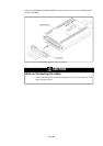
( 23 / 48 )
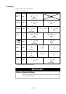
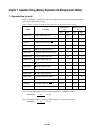
4.4 Data Slicer I/O Signals and OSD Clock I/O Signal Circuits
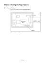
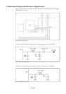
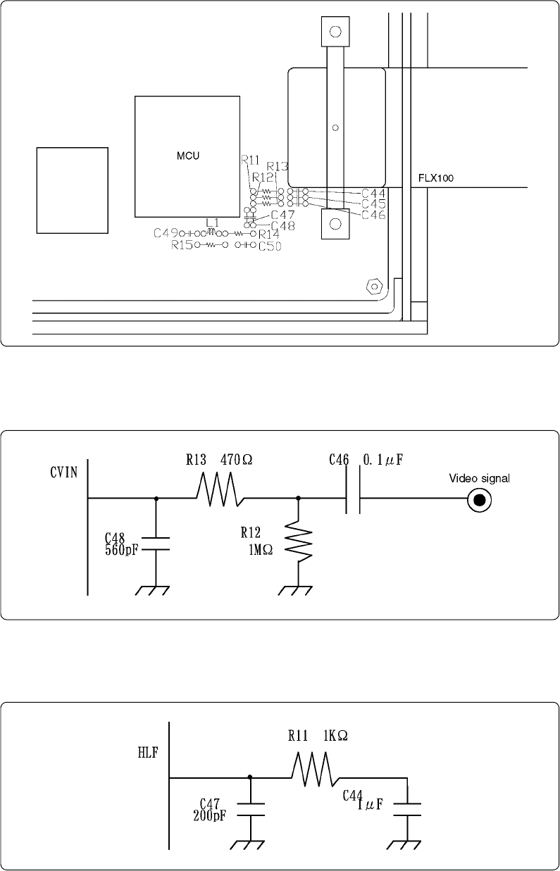
Figure 4.7 shows the layout of the parts on the board and the circuit diagrams used for data slicing
and the OSD clock circuits.
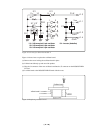
Figure 4.8 CVIN signal circuit
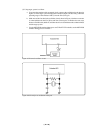
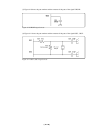
(2) Figure 4.9 shows the part numbers and the constants of the parts of the signal HLF.
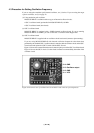
Figure 4.7 Layout of parts
(1) Figure 4.8 shows the part numbers and the constants of the parts of the signal CVIN.
Figure 4.9 HLF signal circuit