


( 59 / 78 )
(4) Timing Requirements
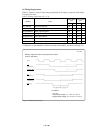
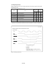
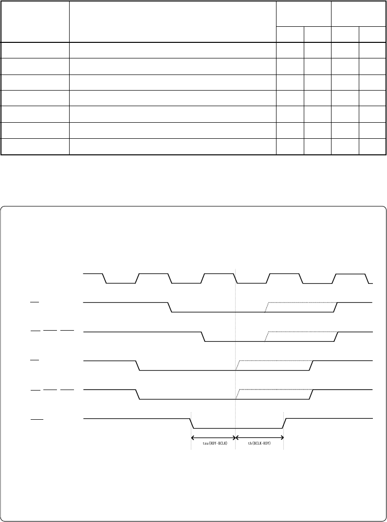
Table 5.9, Figures 5.9 and 5.10 show timing requirements in the memory expansion mode and the
microprocessor mode.
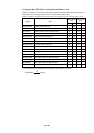
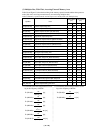
Table 5.9 Timing requirements (VCC = 3 V)
*1 Minimum 7 ns (The definition is different from that of actual MCUs. For details, see Figure 5.10.)
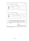
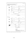
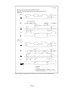
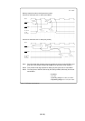
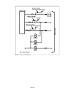
Figure 5.9 Timing requirements
VCC = 3 V
Memory expansion mode and microprocessor mode
(only with wait)
BCLK
RD
(separate bus)
RD
(multiplex bus)
RDY input
WR, WRL, WRH
(separate bus)
WR, WRL, WRH
(multiplex bus)
Conditions:
• V
CC = 3 V
• Input timing voltage: VIL = 0.6 V, VIH = 2.4 V
• Output timing voltage: VOL = 1.5 V, VOH = 1.5 V
Tsu (DB-RD)
Tsu (RDY-BCLK)
Tsu (HOLD-BCLK)
Th (RD-DB)
Th (BCLK-RDY)
Th (BCLK-HOLD)
Td (BCLK-HDLA)
Data input setup time
RDY* input setup time
HOLD* input setup time
Data input hold time
RDY* input hold time
HOLD* input hold time
HLDA* output delay time
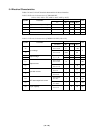
Min.
80
60
80
0
0
0
Max.
100
Min.
80
(*1)
Max.
Actual MCU
[ns]
This product
[ns]
Symbol
Item
See left
See left
See left
See left
See left