


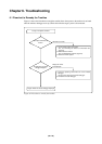


( 72 / 78 )
(4) Data Values of ROM Area at Power-on Are Different
For this product, 04h is written into the ROM area at power-on. Therefore, the data values are different
from those of an actual MCU.
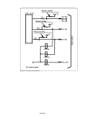
(5) HOLD* control
When inputting "Low" to the HOLD* pin to run into the HOLD state, P00 to P52 will be in the HOLD
state delaying by 2.5 cycles than the actual MCU (see Table 5.5, Figure 5.5, Table 5.9 and Figure
5.10).
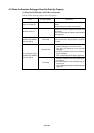
(6) A-D Conversion Values are Different from Expected Values
To use the A-D input group selection function, following settings are required.
1) To select A-D input for port P0
• Set the whole 8-bit direction registers of P107 to P100 to input.
• Set P107 to P100 to no pullup for pullup control resister setting.
• P107 to P100 cannot be used for the input pins of I/O port and key input interrupt functions.
2) To select A-D input for port P2
• Set the whole 8-bit direction registers of P107 to P100 to input.
• Set P107 to P100 to no pullup for pullup control resister setting.
• P107 to P100 cannot be used for the input pins of I/O port and key input interrupt functions.
3) To select A-D input for port P10
• There is no limitation.
As a flexible cable, a pitch converter board and other devices are used between the evaluation MCU
and the target system, some characteristics are slightly different from those of the actual MCU.
Therefore, be sure to evaluate your system with an evaluation MCU. Before starting mask production,
evaluate your system and make final confirmation with an ES (Engineering Sample) version MCU.
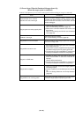
(7) Outputs of ALE, Address and Others are Different from Those of Actual MCUs
1) ALE signal output in accessing the SFR area
2) Address, BHE* and ALE signal outputs in accessing the internal RAM and ROM
3) State of the data bus in the stop mode and wait mode
For details, see Chapter 1 "Note on Differences between Actual MCU and Emulator" (page 14).