R5C841 PCI-CardBus/IEEE 1394/SD Card/Memory Stick/xD/ExpressCard Data Sheet
12345 2004 REV. 1.10 3-12
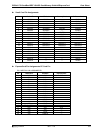
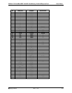
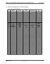
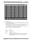
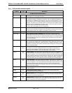
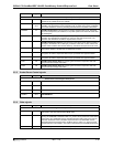
3.3.1 PCI Local Bus interface signals
Pin Name Type Description
PCI Bus Interface Pin Descriptions
PCICLK IN PCI CLOCK: PCICLK provides timing for all transactions on PCI. All other PCI signals
are sampled on the rising edge of PCICLK.
CLKRUN# I/O (OD) PCI CLOCK RUN: This signal indicates the status of PCICLK and an open drain output
to request the starting or speeding up of PCICLK. This pin complies with Mobile PCI
specification. If CLKRUN# is not implemented, then this pin should be tied low. In this
case, CardBus clock is controlled by setting of StopClock bit included Socket Control
Register. This signal has no meaning for the PC Card16 Cards, the CardBus Cards that
does not support CCLKRUN# and not insert Cards to socket. During PCI bus reset is
asserted, this pin placed in a high-impedance state.
And also, refer to the chapter 4.21 for the LED output.
PCIRST# IN PCI RESET: This input is used to initialize all registers, sequences and signals of the
R5C841 to their reset states. PCIRST# causes the R5C841 to place all output buffers in
a high-impedance state. The negation of PCIRST# requires no-bounds.
AD [31:0] I/O ADDRESS AND DATA: Address and Data are multiplexed on the same PCI pins.
C/BE [3:0]# I/O BUS COMMAND AND BYTE ENABLES: Bus Command and Byte Enables are
multiplexed on the same PCI pins. During the address phase of transaction, C/BE [3:0]#
define the bus command. During the data phase C/BE [3:0]# are used as Byte Enables.
The Byte Enables are valid for the entire data phase and determine which byte lanes
carry meaningful data.
PAR I/O PARITY: Parity is even parity across AD [31:0] and C/BE [3:0]#. PAR is stable and valid
one clock after the address phase. For data phases, PAR is stable and valid one clock
after either IRDY# is asserted on a write transaction or TRDY# is asserted on a read
transaction. The master drives PAR for address and write data phases; the target drives
PAR for read data phases.
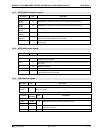
FRAME# I/O
s/h/z
CYCLE FRAME: This signal is driven by the current master to indicate the beginning
and duration of an access. FRAME# is asserted to indicate a bus transaction is
beginning. While FRAME# is asserted, data transfers continue. When FRAME# is
deasserted, the transaction is in the final data phase or has complete.
TRDY# I/O
s/h/z
TARGET READY: This signal indicates the initialing agent‘s ability to complete the
current data phase of the transaction. TRDY# is used in conjunction with IRDY#. A data
phase is completed on any clock both TRDY# and IRDY# are sampled asserted. During
a read, TRDY# and IRDY# are sampled asserted. During a read, TRDY# indicates that
valid data is present on AD [31:0]. During a write, it indicates the target is prepared to
accept data. Wait cycles are inserted both IRDY# and TRDY# are asserted together.
IRDY# I/O
s/h/z
INITIATOR READY: This signal indicates the initiating agent‘s ability to complete the
current data phase of the transaction. IRDY# is used in conjunction with TRDY#. A data
phase is completed on any clock both TRDY# and IRDY# are sampled asserted. During
a write, IRDY# indicates that valid data is present on AD [31:0]. During a read, it
indicates the target is prepared to accept data. Wait cycles are inserted both IRDY# and
TRDY# are asserted together.
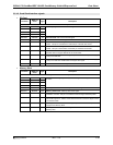
STOP# I/O
s/h/z
STOP: This signal indicates the current target is requesting the master to stop the
current transaction.
IDSEL IN INITIALIZATION DEVICE SELECT: This signal is used as chips select during
configuration read and write transactions.
DEVSEL# I/O
s/h/z
DEVICE SELECT: When actively driven, indicates the driving device has decoded its
address as the target of the current access. As an input, DEVSEL# indicates whether
any device on the bus has been selected.
PERR# I/O
s/h/z
PARITY ERROR: This signal is only for the reporting of data parity errors during all PCI
transactions except a Special Cycle. The R5C841 drives this output active “low” if it
detects a data parity error during a write phase.


