R5C841 PCI-CardBus/IEEE 1394/SD Card/Memory Stick/xD/ExpressCard Data Sheet
12345 2004 REV. 1.10 5-1
5 ELECTRICAL CHARACTERISTICS
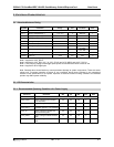
5.1 Absolute Maximum Rating
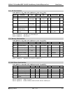
Symbol Parameter Range Unit Condition Note
Vcc 1 Supply Voltage Range 1 -0.3 ~ 2.5 V GND=0V 1
Vcc 2 Supply Voltage Range 2 -0.3 ~ 4.6 V GND=0V 2
Vte1 Voltage on Any Pin -0.3 ~ 5.8 V GND=0V 4
Vte2 Voltage on Any Pin -0.3 ~ 4.6 V GND=0V
Topr Ambient Temperature under bias -40 ~ 85 ºC
Tstg Storage Temperature Range -55 ~ 125 ºC
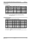
ESD1 Human Body Model
±2.0
kV
C=100pF
R=1.5kΩ
ESD2 Charged Device Model
±1.0
kV
LATUP Latch-up
±100
mA 5ms 3
Note 1: Applied for VCC_ROUT.
Note 2: Applied for VCC_RIN, VCC_3V, VCC_PCI3V and VCC_MD3V and AVCC_PHY3V.
Note 3: The clamping voltage of the trigger pulse power source should be below a value of Vte.
Note 4: Applied for all of Digital pins
Note: Stresses above those listed may cause permanent damage to system components. These are stress
ratings only. Functional operation at these or any conditions above those indicated in the operational
sections of this specification is not implied. Exposure to absolute maximum rating conditions for extended
periods may affect system reliability.
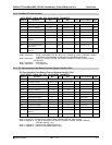
5.2 DC Characteristics
5.2.1 Recommended Operating Conditions for Power Supply
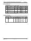
Power Pin Parameter Min Typ Max Unit Note
VCC_PCI3V Supply Voltage for PCI interface
(3.3V Operation)
3.0 3.3 3.6 V
VCC_RIN Supply Voltage for Regulator 3.0 3.3 3.6 V
VCC_RIN,
VCC_ROUT
Supply Voltage for Core Logic
(Disabled regulator: 1.8V Operation)
1.65 1.8 1.95 V
VCC_3V Supply Voltage for System and
Card Interface Signals
3.0 3.3 3.6 V
VCC_MD3V Supply Voltage for Media interface
block
3.0 3.3 3.6 V
AVCC_PHY3V Supply Voltage for Cable interface
block
3.0 3.3 3.6 V


