R5C841 PCI-CardBus/IEEE 1394/SD Card/Memory Stick/xD/ExpressCard Data Sheet
12345 2004 REV.1.10 4-25
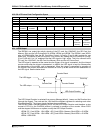
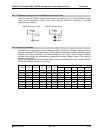
For example, when 53h is written in wrData of the PHY Control register (bit 6, 4, 1, and 0 are set
to “1”), 53h is written in the PHY Register as they are (bit 1, 3, 6, and 7 are set to “1”). Access to
Contender bit, Power_class field, and Disable bit for Port0/Port1 in the 1394 PHY register is
enabled through the PHY Shadow register (99h) in the 1394 configuration register space. Refer
to the PHY Shadow register in the Registers Description for details.
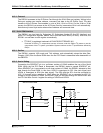
4.22.5 Clock Circuit
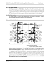
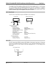
The PHY block of the R5C841 requires 24.576MHz of clock frequency.
Crystal OSC. External Clock Driver
R5C841 R5C841
XO XI XO XI
10pF 10pF OPEN
(±5%) (±5%)
Recommended Conditions
Crystal Oscillator
Normal Frequency : 24.576MHz
Frequency Tolerance : ±50ppm(at 25°C)
Temperature stability : ±50ppm(reference to 25°C)
Operating Temperature Range : -20~70°C
Load Capacitance : 10pF
Driver Level : 0.1mW
Equivalent Series Resistance : 50ohm Max
Insulation resistance : 500M ohm Min (at DC100V±15V)
Shunt Capacitance : 7.0pF Max
External Clock Driver
Normal Frequency : 24.576MHz
Frequency Tolerance : ±50ppm(at 25°C)
4.22.6 PLL
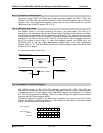
The PHY block of the R5C841 produces 393.216MHz of the internal clock that is 16 times as
long as the 24.576MHz produced by the internal PLL circuit. Setting the Sleep Mode of the PHY
block can stop the PLL circuit. Refer to the Power Management (Ch. 4.11) for settings of the
Sleep Mode.
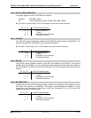
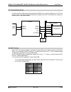
PLL External Circuit
R5C841
FIL0
0.01uF
AGND


