R5C841 PCI-CardBus/IEEE 1394/SD Card/Memory Stick/xD/ExpressCard Data Sheet
12345 2004 REV. 1.10 3-16
Pin Name Type Description
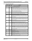
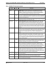
CardBus PC Card Interface Pin Descriptions (Continued)
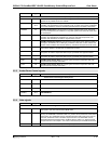
CGNT#
OUT
CardBus Grant: This signal indicates to the agent that access to the bus has been
granted. Every master has its own CGNT#.
CPERR#
I/O
s/h/z
CardBus Parity Error: This signal is only for the reporting of data parity errors during all
CardBus Card transactions except a Special Cycle. An agent cannot report a CPERR#
until it has claimed the access by asserting CDEVSEL# and completed a data phase.
CSERR#
IN
CardBus System Error: This signal is for reporting address parity errors, data parity
errors on the Special Cycle command, or any other system error where the result could
be catastrophic.
CINT#
IN
CardBus Interrupt Request: This signal is an input signal from CardBus card. It is level
sensitive, and asserted low (negative true), using an open drain output driver. The
assertion and deassertion of CINT# is asynchronous to CCLK.
CSTSCHG
IN
CardBus Card Status Change: This signal is an input signal used to alert the system to
changes in the READY, WP, or BVD [2:1] conditions of the card. It is also used for the
system and/or CardBus card interface Wake up. CSTSCHG is asynchronous to CCLK.
CAUDIO
IN
CardBus Card Audio: This signal is a digital audio input signal from a CardBus Card to
the system’s speaker. CAUDIO has no relationship to CCLK.
CCD1#
IN
CardBus Card Detect 1: CCD [2:1]# pins are used to detect the card insertion. CCD
[2:1]# pins are used in conjunction with CVS [2:1] to decode card type information.
CCD2#
IN
CardBus Card Detect 2: CCD [2:1]# pins are used to detect the card insertion. CCD
[2:1]# pins are used in conjunction with CVS [2:1] to decode card type information.
CVS1
I/O
CardBus Card Voltage Sense 1: CVS [2:1] pins are used in conjunction with CCD
[2:1]# to decode card type information.
CVS2
I/O
CardBus Card Voltage Sense 2: CVS [2:1] pins are used in conjunction with CCD
[2:1]# to decode card type information.
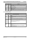
3.3.5 Socket Power Control signals
Pin Name Type Description
Socket Power Control Signal Descriptions
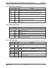
VCC5EN#
OUT
VCC 5V ENABLE:
VCC3EN#
OUT
VCC 3.3V ENABLE:
VPPEN0
OUT
VPP ENABLE 0:
VPPEN1
OUT
VPP ENABLE 1:
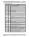
3.3.6 Other signals
Pin Name Type Description
Other Signals Descriptions
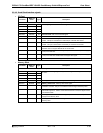
SPKROUT I/O
SPEAKER OUTPUT: This signal is a digital audio output from SPKR#, and Connecting
this signal to pull-down sets the Serial ROM mode.
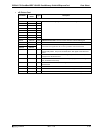
HWSPND# IN
Hardware Suspend: This signal works as HWSPND# input. PCIRST# is not accepted
as long as HWSPND# is asserted so that VCC_PCI3V can be powered off. When Serial
IRQ mode is set, HWSPND# must be asserted after Serial IRQ mode on the chip-set
has been deasserted. When Hardware Suspend mode is off, HWSPND# must be
deasserted before Serial IRQ mode is enabled. When a power is on, follow the reset
sequence shown in the chapter 4.10 in order to confirm the input of PCIRST# and PCLK.
TEST IN
TEST: This signal is a test mode pin. Usually, this pin must be tied low.


