R5C841 PCI-CardBus/IEEE 1394/SD Card/Memory Stick/xD/ExpressCard Data Sheet
12345 2004 REV. 1.10 3-20
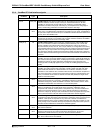
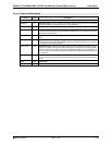
3.3.11 Power and GND signals
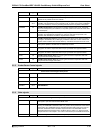
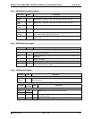
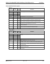
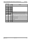
Pin Name Type Description
Power Pin Descriptions
REGEN# IN
Regulator Enable: This pin controls an internal regulator. Setting this pin to ‘Low’ enables
the internal regulator, and setting this pin to ‘High’ disables it.
VCC_PCI3V PWR
PCI VCC: Power Supply pins for the PCI interface signals. This pin can be powered at 3.3V.
VCC_3V PWR
3V VCC : This supply pin is connected to 3.3V. This pin must not be off on the suspend
mode because of the power supply for PME# and GBRST#. This pin supplies for a socket of
the PC Card Controller also.
VCC_MD3V PWR
Media VCC: Power Supply pins for the Media interface signals. This pin can be powered at
3.3V.
VCC_RIN PWR
Regulator Input: Power supply input pins for an internal regulator. This pin is connected to
3.3V when an internal regulator is enabled, and to the same power as that of VCC_ROUT
(1.8V) when the regulator is disabled.
VCC_ROUT PWR
Regulator Output: Power supply output pins for an internal regulator and power supply
pins for the internal core logic. This pin is powered as an output from an internal regulator
and as an input to the core logic when an internal regulator enabled, and connected to 1.8V
as input to the core logic when the regulator disabled. Add bypass condensers between this
pin and GND.
AVCC_PHY3V PWR
1394 PHY VCC: Power supply for PHY analog block. This pin can be powered at 3.3V. Thi
s
pin must not be off on the suspend mode because of the power supply for Cable interface
block.
GND PWR
Digital GND:
AGND PWR
Analog GND:


