R5C841 PCI-CardBus/IEEE 1394/SD Card/Memory Stick/xD/ExpressCard Data Sheet
12345 2004 REV.1.10 4-3
4.3.2 VGA Support
The R5C841 supports accesses to the CardBus interface bridge and the VGA compatible devices
that is downstream of the bridge. When the VGA Enable bit in the Bridge Control register is set,
the R5C841 positively decodes and forwards accesses to VGA frame buffer addresses and I/O
accesses to VGA registers from PCI to CardBus interface. The address range is as follows.
Memory address : 0A0000h to 0BFFFFh
I/O address : AD[9:0] = 3B0h to 3BBh, and 3C0h to 3DFh
(inclusive of ISA address aliases - AD[15:10] are not decoded.)
And also, the R5C841 can forward only write transaction to the VGA Palette register of the
following ranges.
Palette address : AD [9:0] = 3C6h, 3C8h, and 3C9h
(Inclusive of ISA address aliases - AD [15:10] are not decoded.)
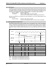
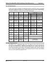
4.4 16-bit Card Interface Timing Control
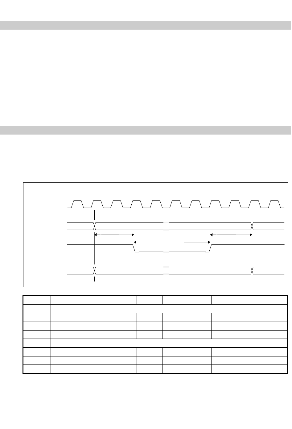
The R5C841 generates the timing of address, data, and command for the 16-bit Card interface.
Each timing is set in a timer granularity of PCI clock as shown below. When 16-bit I/O enhanced
Timing or 16-bit Memory Enhanced Timing bit in each socket control register space is cleared,
the default timing is selected regardless of the I/O Win 0-1 Enhanced Timing bit or Memory
Enhanced Timing bit. Default timing is selected when the value smaller than the minimum value is
set.
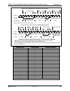
16-bit Card Signal Timing Example
CDATA
OE#, WE#
IOW#, IOR#
CADR,REG#
Data
A
ddress Setup Time
Command Active Time
PCICLK
A
ddress Hold Time
Symbol Parameter Min Max Default Unit
I/O Read/ Write
Tsu Address Setup Time 2 7 3 PCI Clocks (Typ=30ns)
Tpw Command Active Time 3 31 6 PCI Clocks (Typ=30ns)
Thl Address Hold Time 1 7 1 PCI Clocks (Typ=30ns)
Memory Read/ Write
Tsu Address Setup Time 1 7 3 (4) Note 1 PCI Clocks (Typ=30ns)
Tpw Command Active Time 3 31 6 (8or18) Note 2 PCI Clocks (Typ=30ns)
Thl Address Hold Time 1 7 1(2) Note 3 PCI Clocks (Typ=30ns)
Note1 : 4PCI clocks for 3.3v card attribute memory access.
Note2 : 8 PCI clocks for 5v card attribute memory access.
18 PCI clocks for 3.3v card attribute memory access.
Note3 : 2PCI clocks for 3.3v card attribute memory access.


