R5C841 PCI-CardBus/IEEE 1394/SD Card/Memory Stick/xD/ExpressCard Data Sheet
12345 2004 REV.1.10 4-13
4.13 ZV port Interface
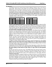
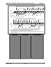
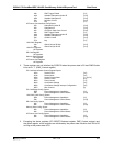
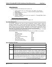
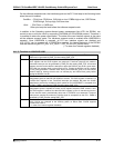
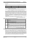
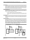
The R5C841 has the Bypass type ZV port interface. On the 16-bit interface, when ZV port Enable
bit of either the Misc Control 1 register (82Fh) or the PC Card Misc Control 2 register (A0h) is
enabled, CADR [25:6], IOIS16#, INPACK#, SPKR# are assigned to ZV port input signal as shown
in the below diagram.
The R5C841 has no on chip buffer for the ZV port interface. So if ZV port is enabled, the signals
for ZV port such as CADR [25:4] will be “Hi-Z” or “Input disable” and they will be reconfigured for
the ZV port interface. The R5C841 outputs the control signal for the external buffer, which is used
to switch sockets, so that the buffer control for switching sockets is enabled.
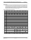
16 bit Interface
Signal Name
ZV Port Interface
Signal Name
ZV Port
card I/O
1
Comments
A10 HREF
O Horizontal Sync to ZV Port
A11 VSYNC
O Vertical Sync to ZV Port
A9 Y0
O Video Data to ZV Port YUV:4:2:2 format
A8 Y2
O Video Data to ZV Port YUV:4:2:2 format
A13 Y4
O Video Data to ZV Port YUV:4:2:2 format
A14 Y6
O Video Data to ZV Port YUV:4:2:2 format
A16 UV2
O Video Data to ZV Port YUV:4:2:2 format
A15 UV4
O Video Data to ZV Port YUV:4:2:2 format
A12 UV6
O Video Data to ZV Port YUV:4:2:2 format
A7 SCLK
O Audio SCLK PCM Signal
A6 MCLK
O Audio MCLK PCM Signal
A[5:4] RESERVED
RFU Put in three state by Host Adapter
No connection in PC Card
A[3:0] ADDRESS[3:0]
I Used for accessing PC Card
IOIS16# PCLK
O Pixel Clock to ZV Port
A17 Y1
O Video Data to ZV Port YUV:4:2:2 format
A18 Y3
O Video Data to ZV Port YUV:4:2:2 format
A19 Y5
O Video Data to ZV Port YUV:4:2:2 format
A20 Y7
O Video Data to ZV Port YUV:4:2:2 format
A21 UV0
O Video Data to ZV Port YUV:4:2:2 format
A22 UV1
O Video Data to ZV Port YUV:4:2:2 format
A23 UV3
O Video Data to ZV Port YUV:4:2:2 format
A24 UV5
O Video Data to ZV Port YUV:4:2:2 format
A25 UV7
O Video Data to ZV Port YUV:4:2:2 format
INPACK# LRCLK
O Audio LRCLK PCM signal
SPKR# SDATA
O Audio PCM Data signal
ZV Port Interface Pin Assignments
1. "I" indicates signal is input to PC Card, "O" indicates signal is output from PC Card.
4.14 Subsystem ID, Subsystem Vendor ID
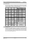
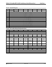
The R5C841 supports Subsystem ID and Subsystem Vendor ID to meet PC98/99/2001 Design
Requirements. There are three ways to write into the Subsystem ID and the Subsystem Vendor
ID registers from the system through BIOS.
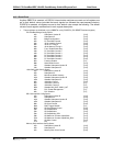
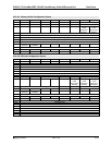
1. Write Enable bit (Card: bit6 in the PC Card Misc Control, 1394: bit4 in the 1394 Misc
Control 2, SD: bit0 in the Key, Memory Stick: bit0 in the Key, xD Picture Card: bit0 in the
Key) control method.
The BIOS can turn this bit on, change the Subsystem IDs, and turn it off.


