


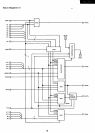
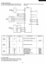
To read the contents
of
a
VRAM
character, the
CPU
sends
out
the relevant address. When
RD
is forced low, the
data
is
then read
via
the bidirectional buffer LS245.
However, the address range
$0000
through $DFFF must
be addressed in order to access
all
the
VRAM.
This address
change
is
carried
out
inside the custom
LSI
with the OUT
command described later.
Accessing
of
the
VRAM
is carried
out
within the blinking
period (BLNK
= "H").
If
BLNK =
"L",
then
WAIT
is
applied to the
CPU
(WA
= "L").
The blanking period discussed here
is
the period that
BLNK
is
in high level.
High
period
of
the BLNK signal
is
so
designed that it
is
shorter than the low period
of
HBLK (horizontal blanking
period).
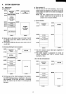
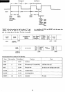
HBLK
versus
BLNK
HBLK~
,
BLNK--,L.
____________
~--~I
!
~
I:
L"I----
, 1
I'
-:
l--
2.165081-1S
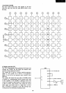
Display period
The data written in the
VRAM
is
sent
to
the
CG
ROM,
character
by
character based on the display address counter
located inside the custom LSI, to become the
CG
address
data (VRAM-l data). Also, the data
of
VRAM-2
is
sent
to the LS174, at this point. The
CG
receives the VRAM-l
data and low order address bits (Q-Q3).
It
is
then sent to
the shift register LS165 after being converted into the
8-bit parallel character row data. The shift register converts
this signal into serial data and it
is
added to the color
matrix circuit along with the data from the LS174 to
become the R.G.B.
CVIDEO signal.
Po
- PlO: These are
VRAM
addresses
that
represent the
character position
on
the CRT screen.
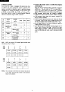
Ql
- Q3: These represent the rows
of
the 8 x 8 dot
character. Row number
is
increased with
HBLK,
and it repeats 0 through 7
as
shown
below. These signals are also generated inside
the custom
LS!.
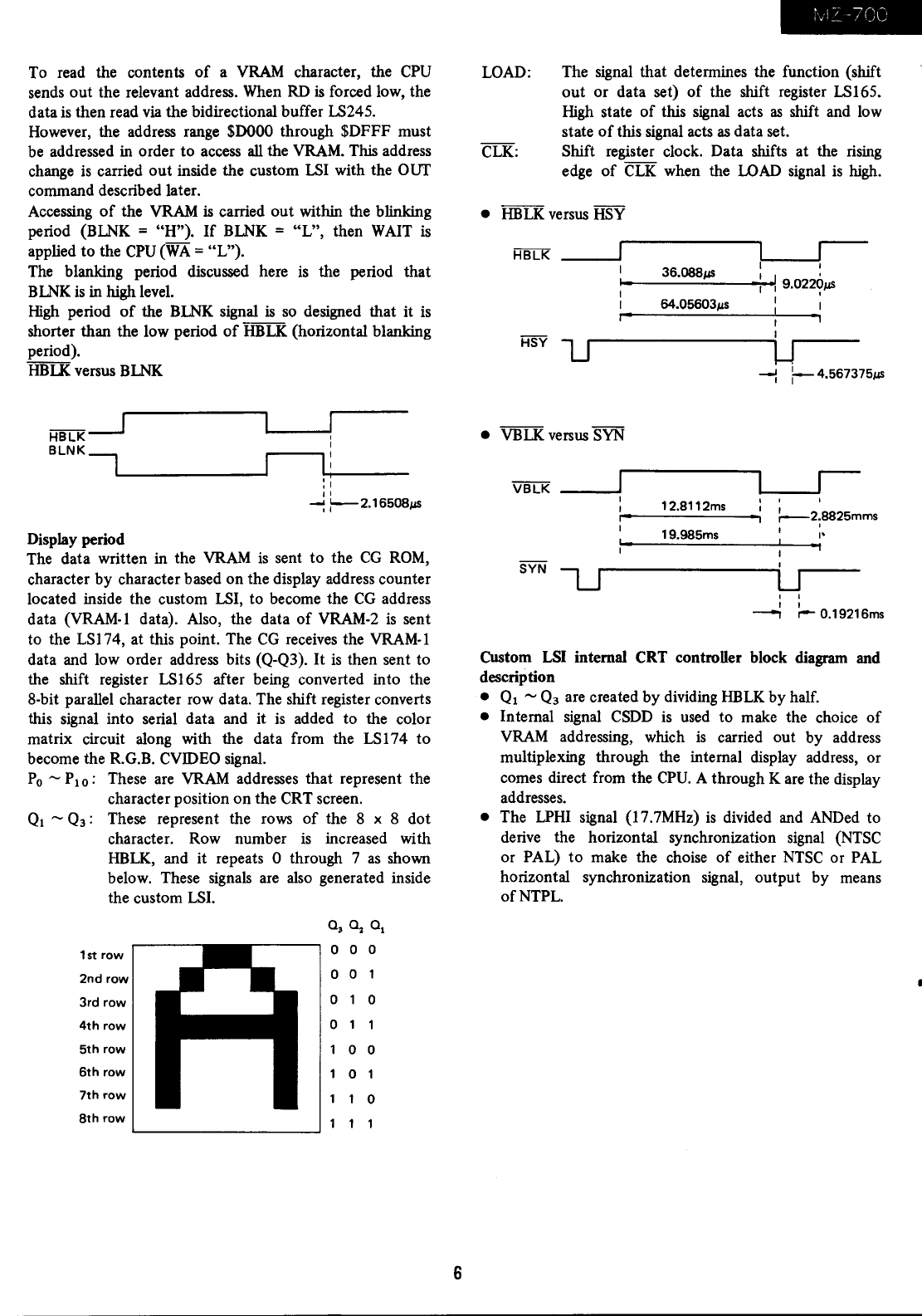
as
a
2
a
1
1st row
0 0
0
2nd
row
0 0
1
3rd row
0
0
4th
row
0
1
1
5th
row
1
0 0
6th
row
1
0 1
7th
row
1
1
0
8th
row
1 1
1
6
LOAD:
CLK:
The signal that determines the function (shift
out
or data set)
of
the shift register LS165.
High state
of
this
signal
acts
as
shift and low
state
of
this signal acts
as
data set.
Shift register clock. Data shifts at the rising
edge
of
CLK
when the
LOAD
signal
is
high.
•
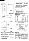
HBLK
versus
HSY
!------Jr---
I 1
36.0881-1S
1 1 '
1-1
-----:...----;I-!'j
9.02201-1S
I I '
1
64.05603/015
1
I·
I
I
1J
W.
-l
:--
4.567375j.1S
• VBLK versus
SYN
VBLK
____
~
~
__
~r---
: 12.8112ms
:;
I
r-I--------·~I
r--2;8825mms
1
~_~1~9=.98==5m~s~
__
~_~.:.
u
, 1
1 1
--,
r--
0.19216ms
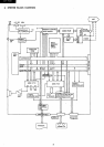
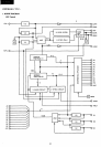
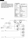
Custom
LSI
internal CRT controUer block diagram and
description
• Ql -
Q3
are created by dividing
HBLK
by half.
• Internal signal
CSDD
is
used to make the choice
of
VRAM
addressing, which
is
carried out by address
muitiplexing through the internal display address, or
comes direct from the
CPU.
A through K are the display
addresses.
• The
LPHI
signal (l7.7MHz)
is
divided and ANDed to
derive the horizontal synchronization signal
(NTSC
or PAL)
to
make the choise
of
either
NTSC
or PAL
horizontal synchronization signal, output by means
ofNTPL.