


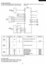

\
,'1Z
-700
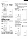
2) Memory controller
In the
MZ·
700, it needs
to
segregate the memory in order
to acheive the above mentioned memory mapping. The
memory controller
is
therefore used
to
perform address
management
of
peripherals assigned
to
the memory such
as
DRAM, monitor
ROM,
video
RAM,
and keyboard. The
bank select method
is
used to switch memory. Memory
selection
is
acheived using the OUT command.
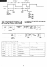
I/O
$0000
$DOOOO
~
l
INHl INH2 INH3
port
$OFFF
$FFFF
$EO
D·RAM
-
L
-
-
$El
-
D-RAM
-
L -
$E2
MONITOR
H
ROM
-
-
-
$E3
-
V·RAM,8255
-
H
-
8253
$E4
MONITOR
V·RAM,8255
H H H
ROM
8253
$E5
-
Prohibited
- -
L
Returns
to
the
$E6
-
state before
-
-
H
prohibitied.
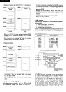
INHl
-
INH3
are custom
LSI
internal signals which cause
the memory map to change.
INH1
INH2
INH3
INH1
INH2
INH3
H L H H
H H L H
H H H L
I--D-_R:_:_M---I
1--:-.:-:-:---1
I---D-_:_OA_MM----j
I
:::
I
V·RAM V·RAM
D-RAM
L
L
H
D·RAM
D-RAM
D·RAM
H
L
L
ROM
D-RAM
L
H
L
D-RAM
D-RAM
L
L
L
D-RAM
D·RAM
NOTE: The command with which the memory selection
is
to
be
done should not
be
written in the memory
block to be selected.
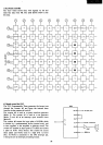
7
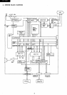
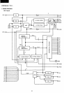
• Custom LSI internal memory controller block diagram
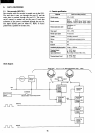
and description
When the above mentioned
OUT command
is
executed,
address
Ao
,..,
A2
is stored in
"FF"
to
create INHl
,..,
INH3,
then
ROM,
VRAM, and
DRAM
may be accessed
against
CPU addressing
on
the basis
of
those INH signals.
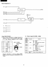
•
RA~
becomes active when the DRAM
is
accessed.
•
CSO
becomes active when the monitor
ROM
is accessed.
•
CSE
becomes active when the memory mapped I/O
(8255,8253)
is accessed.
• CSDN (internal signal) becomes active when the VRAM
is
accessed.
If
in the blnk period, CSDD becomes active.
So
that, the address from the CPU
is
sent
of
Po
,..,
PlO.
•
If
the display period is
on
when accessing the
ROM
or
VRAM, W ATN becomes active.
•
line
address and row address switching signal (LS157
input) when accessing the
RAM
is derived from PHI,
WRN,
MRQN, and RDN.
As
WR
rises before the falling
edge
of
CAS
during the write cycle,
it
becomes an early
cycle.