


IV?
7ce
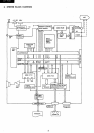
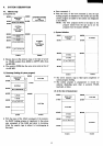
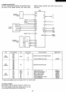
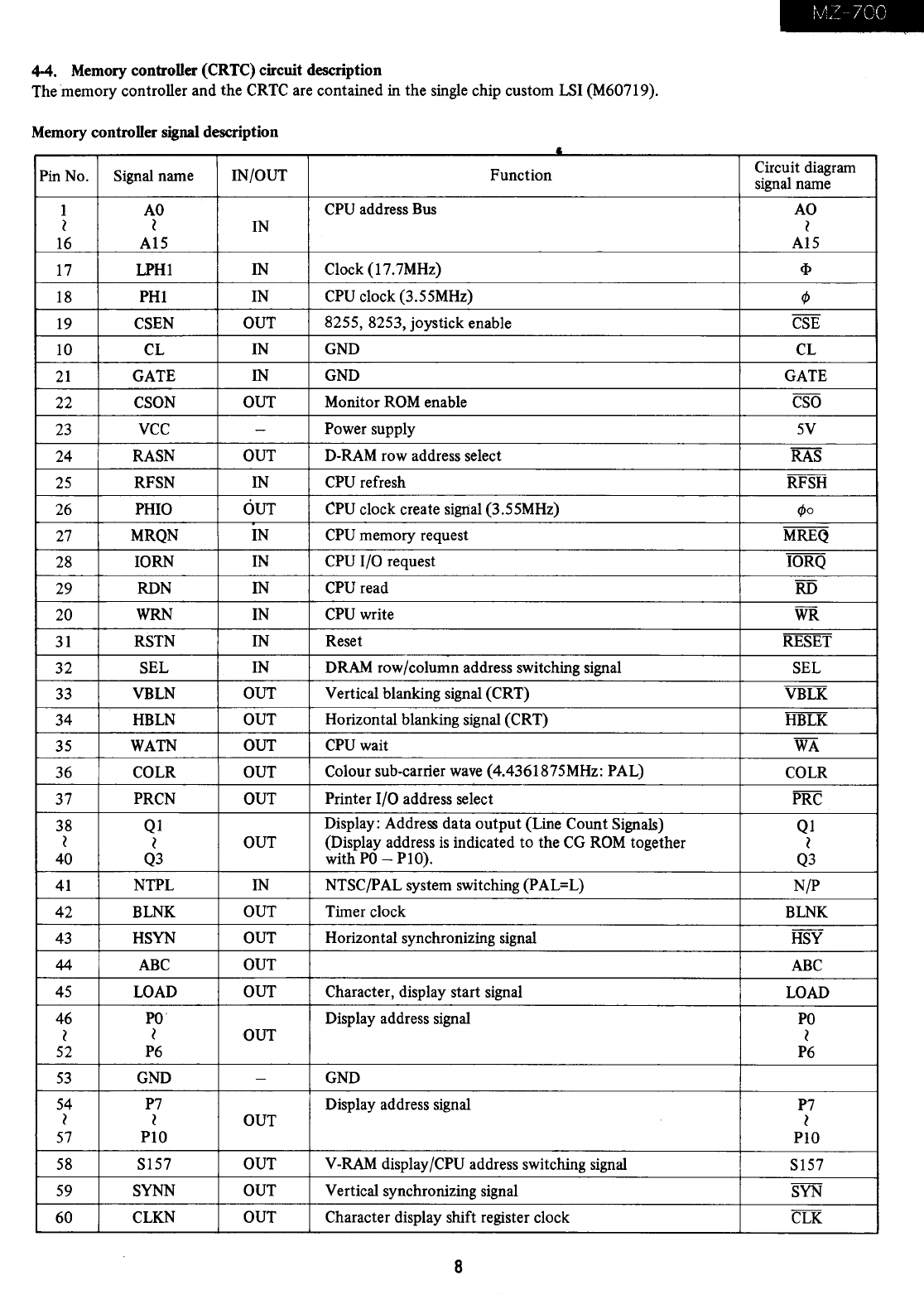
4-4. Memory controller (CRTC) circuit description
The memory controller and
the
CRTC are contained in
the
single chip custom LSI (M60719).
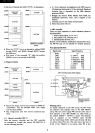
Memory controller signal description
&
Pin No.
Signal name IN/OUT
Function
Circuit diagram
signal name
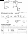
1
AO
CPU address Bus
AO
l
l
IN
l
16
A15
A15
17
LPH1
IN
Clock (17.7MHz)
<I>
18
PHI
IN CPU clock (3.55MHz)
cp
19
CSEN
OUT
8255, 8253, joystick enable
CSE
10 CL
IN GND
CL
21
GATE
IN GND
GATE
22
CSON OUT
Monitor ROM enable
CSO
23
VCC
-
Power supply
5V
24
RASN
OUT
D-RAM row address select
RAS
25
RFSN IN
CPU refresh
RFSH
26
PHIO
OUT
CPU
clock create signal (3.55MHz)
cpo
27
MRQN
IN
CPU memory request MREQ
28
10RN
IN CPU I/O request IORQ
29
RDN IN
CPU read
RD
20
WRN IN
CPU write
WR
31
RSTN
IN Reset
RESET
32
SEL
IN DRAM row/column address switching signal
SEL
33
VBLN
OUT
Vertical blanking signal (CRT)
VBLK
34
HBLN
OUT Horizontal blanking signal (CRT)
HBLK
35 WATN
OUT
CPU
wait
WA
36
COLR
OUT
Colour
sub-carrier wave (4,4361 875MHz: PAL)
COLR
37
PRCN OUT Printer I/O address select
PRC
38
Q1
Display: Address data
output
(Line
Count
Signals)
Ql
l
l
OUT (Display address
is
indicated
to
the
CG ROM together
l
40
Q3
with
PO
- PlO).
Q3
41
NTPL IN NTSC/PAL system switching (PAL=L)
N/P
42
BLNK
OUT Timer clock
BLNK
43
HSYN OUT
Horizontal synchronizing signal
HSY
44
ABC
OUT
ABC
45
LOAD
OUT
Character,
display start signal
LOAD
46
PO
Display address signal
PO
l
~
OUT
l
52
P6
P6
53
GND
-
GND
54
P7 Display address signal
P7
l
l
OUT l
57
PlO
PlO
58
S157 OUT V-RAM display/CPU address switching signal
S157
59
SYNN OUT Vertical synchronizing signal
SYN
60
CLKN
OUT Character
display shift register clock
CLK
8