


9
Sundance Technology ST201 PRELIMINARY draft 2
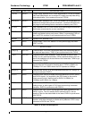
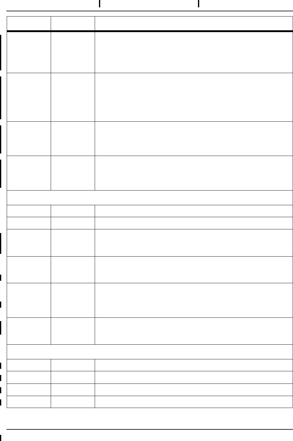
LEDPWRN OUTPUT Power Status LED. (This pin is shared with EA9). The operation of this
pin varies based on the setting in the I/O Registers, AsicCtrl bit 14 (the
LEDMode bit). In Mode 0, LOW when power is applied, and toggling
when frame transmission is in progress. In Mode 1, this pin is always
LOW when power is applied.
LEDLNKN OUTPUT Link Status LED. (This pin is shared with EA10). The operation of this
pin varies based on the setting in the I/O Registers, AsicCtrl bit 14 (the
LEDMode bit). In Mode 0, LOW when a valid link exists, toggling when
frame reception is in progress. In Mode 1, LOW when a valid link
exists, and toggling when either frame transmission or reception is in
progress.
LEDDPLXN OUTPUT Duplex Status LED. (This pin is shared with EA11). This pin operates
independently of the I/O Registers, AsicCtrl bit 14 (the LEDMode bit).
This pin is LOW when the PHY is in full duplex mode, and toggles
when collisions are detected.
LEDSPDN OUTPUT Speed Status LED. (This pin is shared with EA12). This pin operates
independently of the I/O Registers, AsicCtrl bit 14 (the LEDMode bit).
This pin is LOW when the link speed is 100Mbps, and HIGH when the
link speed is 10Mbps.
MISCELLANEOUS
GPIO0 IN/OUT General Purpose Input/Output. (This pin is shared with ED6)
GPIO1 IN/OUT General Purpose Input/Output. (This pin is shared with ED7)
RSTOUT OUTPUT Reset Output, assertion level is programmable (see I/O Registers,
AsicCtrl bit 15). The ST201 will assert RSTOUT when it is being reset.
RSTOUT is intended to be used to reset other circuitry on the adapter.
X25I OSCIN 25MHz Crystal Oscillator Input. The external 25MHz crystal and capac-
itor is connected to the on-chip crystal oscillator circuit through X25I
input. Alternately, X25I can be driven by an external clock source.
X25O OSCOUT 25MHz Crystal Oscillator Output. The external crystal and capacitor is
also connected to the output of the on-chip crystal oscillator circuit
through X25O. When X25I is driven by an external clock source, X25O
should be left unconnected.
CLK25 OUTPUT 25MHz Clock Output. CLK25 carries the reference clock generated by
the on-chip crystal oscillator. This is a free-running and continuous
clock signal.
POWER AND GROUND
VCC (5V) POWER +5 volts power supply.
GND (5V) GROUND +5 volts power return.
VCC (3.3V) POWER +3.3 volts power supply.
GND (3.3V) GROUND +3.3 volts power return.
PIN NAME PIN TYPE PIN DESCRIPTION
TABLE 2: ST201 Pin Descriptions