


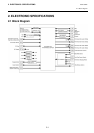

2. ELECTRONICS SPECIFICATIONS EO18-33025
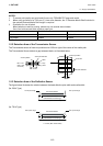
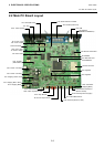
2.3 Description of the Main PC Board
2-6
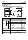
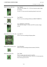
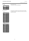
JP4 (Parallel Interfcae): This connector is used for the Parallel (Centronics) interface.
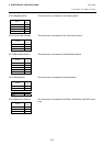
JP7 (Serial Interface): Type: D-Sub 9pin
This connector is used for the Serial (RS-232C) interface.
+5V is output from the pin 1.
The TXD signal is a serial signal and output from the pin 2.
The RXD signal is a serial signal and input into the pin 3.
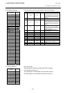
Pin SPP Mode Nibble Mode I/O Function
1 Strobe N/A I
A low on this line indicates that there
are valid data at the host. When this
pin is de-asserted, the +ve clock edge
should be used to shift the data into
the device.
2-9 Data 0-7 N/A I Data Bus. Single-directional.
10 Ack N/A O
A low on this line indicates that there
are valid data at the Device. When this
pin is de-asserted, the +ve clock edge
should be used to shift the data into
the host.
11 Busy N/A Ot
When in reverse direction, a high
indicates data, while a low indicates a
command cycle. In forward direction, it
functions as PtrBusy.
12 Paper Out / End N/A O
When low, device acknowledges
reverse request.
13 Select N/A O Extensibility flag
14 Ground N/A GND Ground
15 No Defined N/A N/A
16-17 Ground N/A GND Ground
18 No Defined N/A N/A
19-30 Ground N/A GND Ground
31 No Defined N/A N/A
32 Error / Fault N/A O
A low set by the device indicates that
the reverse data is available
33-35 Ground N/A GND Ground
36 No Defined N/A N/A
Signal
Pin
No.
Strobe 1
Data0 2
Data1 3
Data2 4
Data3 5
Data4 6
Data5 7
Data6 8
Data7 9
Ack 10
Busy 11
Paper Out / End 12
Select 13
GND 14
No Defined 15
GND 16
GND 17
No Defined 18
GND 19
GND 20
GND 21
GND 22
GND 23
GND 24
GND 25
GND 26
GND 27
GND 28
GND 29
GND 30
No Defined 31
Error / Fault 32
GND 33
GND 34
GND 35
No Defined 36
Signal
Pin
No.
+5 V 1
TXD 2
RXD 3
CTS 4
GND 5
RTS 6
N/C 7
RTS 8
N/C 9